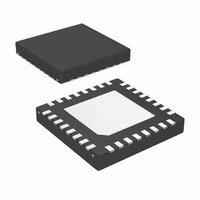
LMH1982SQE/NOPB National Semiconductor, LMH1982SQE/NOPB Datasheet - Page 29

LMH1982SQE/NOPB
Manufacturer Part Number
LMH1982SQE/NOPB
Description
IC CLK GEN MULTI RATE VID 32-LLP
Manufacturer
National Semiconductor
Type
Clock Generatorr
Datasheet
1.LMH1982SQENOPB.pdf
(34 pages)
Specifications of LMH1982SQE/NOPB
Applications
Displays, Projectors, Receivers
Mounting Type
Surface Mount
Package / Case
32-LLP
For Use With
LMH1982SQEEVAL - BOARD EVAL FOR LMH1982SQE
Lead Free Status / RoHS Status
Lead free / RoHS Compliant
Other names
LMH1982SQETR
1's loop response. For more information on setting the loop
response, see section 7.0 LOOP RESPONSE .
To minimize lock time, using a large or maximum I
result in faster PLL settling time due to a wider loop band-
width. Once phase lock has been achieved, using a lower
I
rejection due to a narrower loop bandwidth; this can be helpful
to minimize low-frequency input jitter from being transferred
to the output clocks.
Note: An ICP1 value
ed
Examples:
Bits 7-5: Reserved (RSV)
These RSV bits are reserved. When writing to this register,
only write the default data to the RSV bits as specified in Table
8.
Register 14h
CP1
ICP1 register range = 0 to 31d; 0 to 2d are not recommend-
I
ICP1 = 8d (default) gives I
ICP1 = 31d (max) gives I
CP1
(that yields sufficient stability) can provide good input jitter
I
bility and performance (e.g. wander, loss of lock) due to loop filter
charge leakage and other secondary factors; therefore, it is not rec-
ommended to use an ICP1 value less than 2d nor use an insufficient
DF setting.
CP1
current = ICP1 x 31.25 µA (nominal current step)
setting or low damping factor (DF) can cause reduced PLL sta-
≤
2 corresponds to an I
CP1
CP1
= 968.75 µA nominal
= 250 µA nominal
CP1
current
≤
62.5 µA. A low
CP1
can
29
Bits 3-0: PLL 3 Charge Pump Current Control (ICP3)
ICP3 can be programmed to specify the charge pump current
for PLL 3, which generates the 74.176 and 148.35 MHz HD
clock outputs. Reducing the value of ICP3 will reduce the PLL
3 charge pump current and lower its loop bandwidth at the
expense of reduced PLL stability. An ICP3 value of 0 should
not be programmed since this corresponds to 0 µA nominal
current, which will cause PLL 3 to lose phase lock or otherwise
be unstable.
Bit 7-4: PLL 2 Charge Pump Current Control (ICP2)
ICP2 can be programmed to specify the charge pump current
for PLL 2, which generates the 74.25 and 148.5 MHz HD clock
outputs. Reducing the value of ICP2 will reduce the PLL 2
charge pump current and lower its loop bandwidth at the ex-
pense of reduced PLL stability. An ICP2 value of 0 should not
be programmed since this corresponds to 0 µA nominal cur-
rent, which will cause PLL 2 to lose phase lock or otherwise
be unstable.
9.10 Reserved Registers
Register 15h-1Fh
This register is reserved. Do not program any data to these
registers.
ICP3 register range = 0 to 15d
ICP2 register range = 0 to 15d
www.national.com


