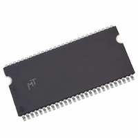
MT48LC32M16A2P-75 L:C TR Micron Technology Inc, MT48LC32M16A2P-75 L:C TR Datasheet - Page 13

MT48LC32M16A2P-75 L:C TR
Manufacturer Part Number
MT48LC32M16A2P-75 L:C TR
Description
IC SDRAM 512MBIT 133MHZ 54TSOP
Manufacturer
Micron Technology Inc
Datasheet
1.MT48LC64M8A2TG-75C_TR.pdf
(68 pages)
Specifications of MT48LC32M16A2P-75 L:C TR
Format - Memory
RAM
Memory Type
SDRAM
Memory Size
512M (32Mx16)
Speed
133MHz
Interface
Parallel
Voltage - Supply
3 V ~ 3.6 V
Operating Temperature
0°C ~ 70°C
Package / Case
54-TSOP II
Lead Free Status / RoHS Status
Lead free / RoHS Compliant
Register Definition
Mode Register
Burst Length (BL)
Burst Type
PDF: 09005aef809bf8f3/Source: 09005aef80818a4a
512MbSDRAM.fm - Rev. L 10/07 EN
The mode register is used to define the specific mode of operation of the SDRAM. This
definition includes the selection of BL, a burst type, CL, an operating mode, and a write
burst mode, as shown in Figure 5 on page 14. The mode register is programmed via the
LOAD MODE REGISTER command and will retain the stored information until it is
programmed again or the device loses power.
Mode register bits M0–M2 specify BL, M3 specifies the type of burst (sequential or inter-
leaved), M4–M6 specify CL, M7 and M8 specify the operating mode, M9 specifies the
write burst mode, and M10 and M11 are reserved for future use. Address A12 (M12) is
undefined but should be driven LOW during loading of the mode register.
The mode register must be loaded when all banks are idle, and the controller must wait
the specified time before initiating the subsequent operation. Violating either of these
requirements will result in unspecified operation.
Read and write accesses to the SDRAM are burst oriented, with BL being programmable,
as shown in Figure 5 on page 14. BL determines the maximum number of column loca-
tions that can be accessed for a given READ or WRITE command. Burst lengths of 1, 2, 4,
or 8 locations are available for both the sequential and the interleaved burst types, and a
full-page burst is available for the sequential type. The full-page burst is used in
conjunction with the BURST TERMINATE command to generate arbitrary burst lengths.
Reserved states should not be used because unknown operation or incompatibility with
future versions may result.
When a READ or WRITE command is issued, a block of columns equal to BL is effectively
selected. All accesses for that burst take place within this block, meaning that the burst
will wrap within the block if a boundary is reached. The block is uniquely selected by A1–
A9, A11, A12 (x4); A1–A9, A11 (x8); or A1–A9 (x16) when BL = 2; by A2–A9, A11, A12 (x4);
A2–A9, A11 (x8) or A2–A9 (x16) when the BL = 4; and by A3–A9, A11, A12 (x4); A3–A9, A11
(x8) or A3–A9 (x16) when the BL = 8. The remaining (least significant) address bit(s) is
(are) used to select the starting location within the block. Full-page bursts wrap within
the page if the boundary is reached.
Accesses within a given burst may be programmed either to be sequential or interleaved;
this is referred to as the burst type and is selected via bit M3.
The ordering of accesses within a burst is determined by BL, the burst type and the
starting column address, as shown in Table 4 on page 15.
13
Micron Technology, Inc., reserves the right to change products or specifications without notice.
512Mb: x4, x8, x16 SDRAM
©2000 Micron Technology, Inc. All rights reserved.
Register Definition


