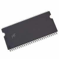
MT48LC32M16A2P-75 L:C TR Micron Technology Inc, MT48LC32M16A2P-75 L:C TR Datasheet - Page 20

MT48LC32M16A2P-75 L:C TR
Manufacturer Part Number
MT48LC32M16A2P-75 L:C TR
Description
IC SDRAM 512MBIT 133MHZ 54TSOP
Manufacturer
Micron Technology Inc
Datasheet
1.MT48LC64M8A2TG-75C_TR.pdf
(68 pages)
Specifications of MT48LC32M16A2P-75 L:C TR
Format - Memory
RAM
Memory Type
SDRAM
Memory Size
512M (32Mx16)
Speed
133MHz
Interface
Parallel
Voltage - Supply
3 V ~ 3.6 V
Operating Temperature
0°C ~ 70°C
Package / Case
54-TSOP II
Lead Free Status / RoHS Status
Lead free / RoHS Compliant
Operations
Bank/Row Activation
Figure 7:
PDF: 09005aef809bf8f3/Source: 09005aef80818a4a
512MbSDRAM.fm - Rev. L 10/07 EN
Activating a Specific Row In a Specific Bank
The procedure for exiting self refresh requires a sequence of commands. First, CLK must
be stable (stable clock is defined as a signal cycling within timing constraints specified
for the clock pin) prior to CKE going back HIGH. When CKE is HIGH, the SDRAM must
have NOP commands issued (a minimum of two clocks) for
required for the completion of any internal refresh in progress.
Upon exiting the self refresh mode, AUTO REFRESH commands must be issued every
7.81µs or less as both SELF REFRESH and AUTO REFRESH utilize the row refresh
counter.
Before any READ or WRITE commands can be issued to a bank within the SDRAM, a row
in that bank must be “opened.” This is accomplished via the ACTIVE command, which
selects both the bank and the row to be activated (see Figure 7).
After opening a row (issuing an ACTIVE command), a READ or WRITE command may be
issued to that row, subject to the
the clock period and rounded up to the next whole number to determine the earliest
clock edge after the ACTIVE command on which a READ or WRITE command can be
entered. For example, a
results in 2.5 clocks, rounded to 3. This is reflected in Figure 8 on page 21, which covers
any case where 2 <
specification limits from time units to clock cycles). A subsequent ACTIVE command to
a different row in the same bank can only be issued after the previous active row has
been “closed” (precharged). The minimum time interval between successive ACTIVE
commands to the same bank is defined by
BA0, BA1
A0–A12
RAS#
CAS#
WE#
CKE
CLK
CS#
HIGH
t
RCD (MIN)/
t
RCD specification of 20ns with a 125 MHz clock (8ns period)
ADDRESS
ADDRESS
BANK
ROW
20
t
t
CK
RCD specification.
Don’t Care
≤
3 (the same procedure is used to convert other
Micron Technology, Inc., reserves the right to change products or specifications without notice.
t
RC.
t
RCD (MIN) should be divided by
512Mb: x4, x8, x16 SDRAM
t
XSR because time is
©2000 Micron Technology, Inc. All rights reserved.
Operations


