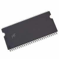
MT48LC32M16A2P-75 L:C TR Micron Technology Inc, MT48LC32M16A2P-75 L:C TR Datasheet - Page 15

MT48LC32M16A2P-75 L:C TR
Manufacturer Part Number
MT48LC32M16A2P-75 L:C TR
Description
IC SDRAM 512MBIT 133MHZ 54TSOP
Manufacturer
Micron Technology Inc
Datasheet
1.MT48LC64M8A2TG-75C_TR.pdf
(68 pages)
Specifications of MT48LC32M16A2P-75 L:C TR
Format - Memory
RAM
Memory Type
SDRAM
Memory Size
512M (32Mx16)
Speed
133MHz
Interface
Parallel
Voltage - Supply
3 V ~ 3.6 V
Operating Temperature
0°C ~ 70°C
Package / Case
54-TSOP II
Lead Free Status / RoHS Status
Lead free / RoHS Compliant
Table 4:
CAS Latency (CL)
PDF: 09005aef809bf8f3/Source: 09005aef80818a4a
512MbSDRAM.fm - Rev. L 10/07 EN
Burst Definition
Notes:
1. For full-page accesses: y = 4,096 (x4); y = 2,048 (x8); y = 1,024 (x16).
2. For BL = 2, A1–A9, A11, A12 (x4); A1–A9, A11 (x8); or A1–A9 (x16) select the block-of-two
3. For BL = 4, A2–A9, A11, A12 (x4); A2–A9, A11 (x8); or A2–A9 (x16) select the block-of-four
4. For BL = 8, A3–A9, A11, A12 (x4); A3–A9, A11 (x8); or A3–A9 (x16) select the block-of-eight
5. For a full-page burst, the full row is selected and A0–A9, A11, A12 (x4); A0–A9, A11 (x8); or
6. Whenever a boundary of the block is reached within a given sequence above, the following
7. For BL = 1, A0–A9, A11, A12 (x4); A0–A9, A11 (x8); or A0–A9 (x16) select the unique column
CL is the delay, in clock cycles, between the registration of a READ command and the
availability of the first piece of output data. The latency can be set to two or three clocks.
If a READ command is registered at clock edge n and the latency is m clocks, the data will
be available by clock edge n + m. The DQs will start driving as a result of the clock edge
one cycle earlier (n + m - 1), and provided that the relevant access times are met, the data
will be valid by clock edge n + m. For example, assuming that the clock cycle time is such
that all relevant access times are met, if a READ command is registered at T0 and the
page (y)
Length
Burst
burst; A0 selects the starting column within the block.
burst; A0–A1 select the starting column within the block.
burst; A0–A2 select the starting column within the block.
A0–A9 (x16) select the starting column.
access wraps within the block.
to be accessed, and mode register bit M3 is ignored.
Full
2
4
8
Starting Column
A2
n = A0–A12/11/9
0
0
0
0
1
1
1
1
–
–
–
–
–
–
–
–
(location 0–y)
Address
A1
A1
–
–
–
0
0
1
1
0
0
1
1
0
0
1
1
A0
A0
A0
0
1
0
1
0
1
0
1
0
1
0
1
0
1
15
Type = Sequential
0-1-2-3-4-5-6-7
1-2-3-4-5-6-7-0
2-3-4-5-6-7-0-1
3-4-5-6-7-0-1-2
4-5-6-7-0-1-2-3
5-6-7-0-1-2-3-4
6-7-0-1-2-3-4-5
7-0-1-2-3-4-5-6
Cn, Cn + 1,
Cn + 4…,
…Cn - 1,
Micron Technology, Inc., reserves the right to change products or specifications without notice.
0-1-2-3
1-2-3-0
2-3-0-1
3-0-1-2
Cn + 3,
Cn + 2
Cn…
0-1
1-0
Order of Accesses Within a Burst
512Mb: x4, x8, x16 SDRAM
©2000 Micron Technology, Inc. All rights reserved.
Type = Interleaved
Register Definition
0-1-2-3-4-5-6-7
1-0-3-2-5-4-7-6
2-3-0-1-6-7-4-5
3-2-1-0-7-6-5-4
4-5-6-7-0-1-2-3
5-4-7-6-1-0-3-2
6-7-4-5-2-3-0-1
7-6-5-4-3-2-1-0
Not supported
0-1-2-3
1-0-3-2
2-3-0-1
3-2-1-0
0-1
1-0


