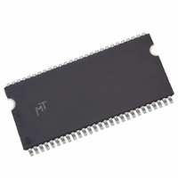
MT48LC32M16A2P-75 L:C TR Micron Technology Inc, MT48LC32M16A2P-75 L:C TR Datasheet - Page 30

MT48LC32M16A2P-75 L:C TR
Manufacturer Part Number
MT48LC32M16A2P-75 L:C TR
Description
IC SDRAM 512MBIT 133MHZ 54TSOP
Manufacturer
Micron Technology Inc
Datasheet
1.MT48LC64M8A2TG-75C_TR.pdf
(68 pages)
Specifications of MT48LC32M16A2P-75 L:C TR
Format - Memory
RAM
Memory Type
SDRAM
Memory Size
512M (32Mx16)
Speed
133MHz
Interface
Parallel
Voltage - Supply
3 V ~ 3.6 V
Operating Temperature
0°C ~ 70°C
Package / Case
54-TSOP II
Lead Free Status / RoHS Status
Lead free / RoHS Compliant
Figure 20:
Figure 21:
PDF: 09005aef809bf8f3/Source: 09005aef80818a4a
512MbSDRAM.fm - Rev. L 10/07 EN
Random WRITE Cycles
WRITE-to-READ
Note:
Note:
COMMAND
COMMAND
Data for a fixed-length WRITE burst may be followed by, or truncated with, a
PRECHARGE command to the same bank (provided that auto precharge was not acti-
vated), and a full-page WRITE burst may be truncated with a PRECHARGE command to
the same bank. The PRECHARGE command should be issued
which the last desired input data element is registered. The auto precharge mode
requires a
truncating a WRITE burst, the DQM signal must be used to mask input data for the clock
edge prior to, and the clock edge coincident with, the PRECHARGE command. An
example is shown in Figure 22 on page 31. Data n + 1 is either the last of a burst of two or
the last desired of a longer burst. Following the PRECHARGE command, a subsequent
command to the same bank cannot be issued until
issued coincident with the first coincident second clock (Figure 22 on page 31). In the
case of a fixed-length burst being executed to completion, a PRECHARGE command
issued at the optimum time (as described above) provides the same operation that
would result from the same fixed-length burst with auto precharge. The disadvantage of
ADDRESS
ADDRESS
Each WRITE command may be to any bank. DQM is LOW.
The WRITE or READ commands may be to any bank. DQM is LOW.
CLK
DQ
CLK
DQ
t
WR of at least one clock plus time, regardless of frequency. In addition, when
BANK,
WRITE
COL n
D
WRITE
BANK,
T0
COL n
n
IN
D
T0
n
IN
Transitioning Data
WRITE
BANK,
COL a
T1
D
n + 1
a
NOP
IN
D
T1
IN
30
BANK,
WRITE
COL x
T2
D
BANK,
x
COL b
READ
IN
T2
Transitioning Data
Don’t Care
WRITE
BANK,
COL m
Micron Technology, Inc., reserves the right to change products or specifications without notice.
T3
D
m
T3
IN
NOP
NOP
D
T4
OUT
b
t
RP is met. The precharge can be
512Mb: x4, x8, x16 SDRAM
Don’t Care
NOP
b + 1
T5
D
OUT
t
WR after the clock edge at
©2000 Micron Technology, Inc. All rights reserved.
Operations


