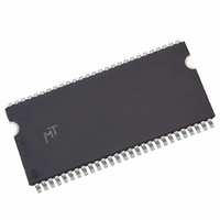
MT48LC32M16A2P-75 L:C TR Micron Technology Inc, MT48LC32M16A2P-75 L:C TR Datasheet - Page 41

MT48LC32M16A2P-75 L:C TR
Manufacturer Part Number
MT48LC32M16A2P-75 L:C TR
Description
IC SDRAM 512MBIT 133MHZ 54TSOP
Manufacturer
Micron Technology Inc
Datasheet
1.MT48LC64M8A2TG-75C_TR.pdf
(68 pages)
Specifications of MT48LC32M16A2P-75 L:C TR
Format - Memory
RAM
Memory Type
SDRAM
Memory Size
512M (32Mx16)
Speed
133MHz
Interface
Parallel
Voltage - Supply
3 V ~ 3.6 V
Operating Temperature
0°C ~ 70°C
Package / Case
54-TSOP II
Lead Free Status / RoHS Status
Lead free / RoHS Compliant
PDF: 09005aef809bf8f3/Source: 09005aef80818a4a
512MbSDRAM.fm - Rev. L 10/07 EN
10. For a READ without auto precharge interrupted by a READ (with or without auto pre-
11. For a READ without auto precharge interrupted by a WRITE (with or without auto pre-
12. For a WRITE without auto precharge interrupted by a READ (with or without auto pre-
13. For a WRITE without auto precharge interrupted by a WRITE (with or without auto pre-
14. For a READ with auto precharge interrupted by a READ (with or without auto precharge),
15. For a READ with auto precharge interrupted by a WRITE (with or without auto precharge),
16. For a WRITE with auto precharge interrupted by a READ (with or without auto precharge),
17. For a WRITE with auto precharge interrupted by a WRITE (with or without auto precharge),
5. A BURST TERMINATE command cannot be issued to another bank; it applies to the bank
6. All states and sequences not shown are illegal or reserved.
7. READs or WRITEs to bank m listed in the Command (Action) column include READs or
8. Concurrent auto precharge: Bank n will initiate the auto precharge command when its
9. Burst in bank n continues as initiated.
represented by the current state only.
WRITEs with auto precharge enabled and READs or WRITEs with auto precharge disabled.
burst has been interrupted by bank m’s burst.
charge), the READ to bank m will interrupt the READ on bank n, CL later (Figure 11 on
page 23).
charge), the WRITE to bank m will interrupt the READ on bank n when registered (Figure 13
and Figure 14 on page 25). DQM should be used one clock prior to the WRITE command to
prevent bus contention.
charge), the READ to bank m will interrupt the WRITE on bank n when registered (Figure 21
on page 30), with the data-out appearing CL later. The last valid WRITE to bank n will be
data-in registered one clock prior to the READ to bank m.
charge), the WRITE to bank m will interrupt the WRITE on bank n when registered
(Figure 19 on page 29). The last valid WRITE to bank n will be data-in registered one clock
prior to the READ to bank m.
the READ to bank m will interrupt the READ on bank n, CL later. The PRECHARGE to bank n
will begin when the READ to bank m is registered (Figure 28 on page 35).
the WRITE to bank m will interrupt the READ on bank n when registered. DQM should be
used two clocks prior to the WRITE command to prevent bus contention. The PRECHARGE
to bank n will begin when the WRITE to bank m is registered (Figure 29 on page 36).
the READ to bank m will interrupt the WRITE on bank n when registered, with the data-out
appearing CL later. The PRECHARGE to bank n will begin after
begins when the READ to bank m is registered. The last valid WRITE to bank n will be data-
in registered one clock prior to the READ to bank m (Figure 30 on page 36).
the WRITE to bank m will interrupt the WRITE on bank n when registered. The PRECHARGE
to bank n will begin after
istered. The last valid WRITE to bank n will be data registered one clock prior to the WRITE
to bank m (Figure 31 on page 37).
t
WR is met, where
41
Micron Technology, Inc., reserves the right to change products or specifications without notice.
t
WR begins when the WRITE to bank m is reg-
512Mb: x4, x8, x16 SDRAM
t
WR is met, where
©2000 Micron Technology, Inc. All rights reserved.
Operations
t
WR


