MA180023 Microchip Technology, MA180023 Datasheet - Page 125
MA180023
Manufacturer Part Number
MA180023
Description
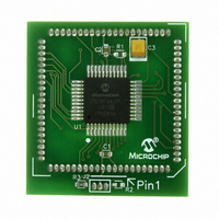
MODULE PLUG-IN PIC18F46J11 PIM
Manufacturer
Microchip Technology
Series
PIC®r
Datasheet
1.MA180023.pdf
(528 pages)
Specifications of MA180023
Accessory Type
Plug-In Module (PIM) - PIC18F46J11
Tool / Board Applications
General Purpose MCU, MPU, DSP, DSC
Mcu Supported Families
PIC18
Supported Devices
Stand-alone Or W/ HPC(DM183022) Or PIC18(DM183032)
Silicon Manufacturer
Microchip
Core Architecture
PIC
Core Sub-architecture
PIC18
Silicon Core Number
PIC18F
Silicon Family Name
PIC18FxxJxx
Lead Free Status / RoHS Status
Lead free / RoHS Compliant
For Use With/related Products
HPC Explorer Board (DM183022) or PIC18 Explorer Board (DM183032)
For Use With
DM183032 - BOARD EXPLORER PICDEM PIC18DM183022 - BOARD DEMO PIC18FXX22 64/80TQFP
Lead Free Status / RoHS Status
Lead free / RoHS Compliant
Available stocks
Company
Part Number
Manufacturer
Quantity
Price
Company:

Part Number:
MA180023
Manufacturer:
Microchip Technology
Quantity:
135


9.0
Depending on the device selected and features
enabled, there are up to five ports available. Some pins
of the I/O ports are multiplexed with an alternate
function from the peripheral features on the device. In
general, when a peripheral is enabled, that pin may not
be used as a general purpose I/O pin.
Each port has three registers for its operation. These
registers are:
• TRIS register (Data Direction register)
• PORT register (reads the levels on the pins of the
• LAT register (Data Latch)
The Data Latch (LAT register) is useful for read-modify-
write operations on the value that the I/O pins are
driving.
Figure 9-1 displays a simplified model of a generic I/O
port, without the interfaces to other peripherals.
FIGURE 9-1:
© 2009 Microchip Technology Inc.
device)
RD LAT
Data
Bus
WR LAT
or PORT
WR TRIS
RD TRIS
RD PORT
Note 1: I/O pins have diode protection to V
I/O PORTS
V
SS
TRIS Latch
Data Latch
D
D
CK
CK
.
GENERIC I/O PORT
OPERATION
Q
Q
Q
EN
EN
D
I/O pin
Buffer
Input
DD
and
(1)
PIC18F46J11 FAMILY
9.1
When developing an application, the capabilities of the
port pins must be considered. Outputs on some pins
have higher output drive strength than others. Similarly,
some pins can tolerate higher than V
9.1.1
The output pin drive strengths vary for groups of pins
intended to meet the needs for a variety of applications.
PORTB and PORTC are designed to drive higher
loads, such as LEDs. All other ports are designed for
small loads, typically indication only. Table 9-1 sum-
marizes the output capabilities. Refer to Section 28.0
“Electrical Characteristics” for more details.
TABLE 9-1:
9.1.2
The voltage tolerance of pins used as device inputs is
dependent on the pin’s input function. Pins that are used
as digital only inputs are able to handle DC voltages up
to 5.5V; a level typical for digital logic circuits. In contrast,
pins that also have analog input functions of any kind
can only tolerate voltages up to V
beyond V
summarizes
Section 28.0 “Electrical Characteristics” for more
details.
TABLE 9-2:
PORTA
PORTD
PORTE
PORTB
PORTC
PORTA<7:0>
PORTB<3:0>
PORTC<2:0>
PORTE<2:0>
PORTB<7:4>
PORTC<7:3>
PORTD<7:0>
Port or Pin
Port
I/O Port Pin Capabilities
DD
PIN OUTPUT DRIVE
INPUT PINS AND VOLTAGE
CONSIDERATIONS
on these pins should be avoided. Table 9-2
Minimum Intended for indication.
the
Drive
High
Tolerated
OUTPUT DRIVE LEVELS
INPUT VOLTAGE LEVELS
Input
5.5V
V
input
DD
Suitable for direct LED drive
levels.
capabilities.
Only V
tolerated.
Tolerates input levels
above V
most standard logic.
DD
Description
. Voltage excursions
DS39932C-page 125
Description
DD
DD
DD
input levels.
input levels
, useful for
Refer
to
Related parts for MA180023
Image
Part Number
Description
Manufacturer
Datasheet
Request
R

Part Number:
Description:
Manufacturer:
Microchip Technology Inc.
Datasheet:
Part Number:
Description:
Manufacturer:
Microchip Technology Inc.
Datasheet:
Part Number:
Description:
Manufacturer:
Microchip Technology Inc.
Datasheet:
Part Number:
Description:
Manufacturer:
Microchip Technology Inc.
Datasheet:
Part Number:
Description:
Manufacturer:
Microchip Technology Inc.
Datasheet:
Part Number:
Description:
Manufacturer:
Microchip Technology Inc.
Datasheet:
Part Number:
Description:
Manufacturer:
Microchip Technology Inc.
Datasheet:
Part Number:
Description:
Manufacturer:
Microchip Technology Inc.
Datasheet: