MA180023 Microchip Technology, MA180023 Datasheet - Page 246
MA180023
Manufacturer Part Number
MA180023
Description
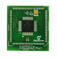
MODULE PLUG-IN PIC18F46J11 PIM
Manufacturer
Microchip Technology
Series
PIC®r
Datasheet
1.MA180023.pdf
(528 pages)
Specifications of MA180023
Accessory Type
Plug-In Module (PIM) - PIC18F46J11
Tool / Board Applications
General Purpose MCU, MPU, DSP, DSC
Mcu Supported Families
PIC18
Supported Devices
Stand-alone Or W/ HPC(DM183022) Or PIC18(DM183032)
Silicon Manufacturer
Microchip
Core Architecture
PIC
Core Sub-architecture
PIC18
Silicon Core Number
PIC18F
Silicon Family Name
PIC18FxxJxx
Lead Free Status / RoHS Status
Lead free / RoHS Compliant
For Use With/related Products
HPC Explorer Board (DM183022) or PIC18 Explorer Board (DM183032)
For Use With
DM183032 - BOARD EXPLORER PICDEM PIC18DM183022 - BOARD DEMO PIC18FXX22 64/80TQFP
Lead Free Status / RoHS Status
Lead free / RoHS Compliant
Available stocks
Company
Part Number
Manufacturer
Quantity
Price
Company:

Part Number:
MA180023
Manufacturer:
Microchip Technology
Quantity:
135


PIC18F46J11 FAMILY
17.4
In Pulse-Width Modulation (PWM) mode, the CCPx pin
produces up to a 10-bit resolution PWM output.
Figure 17-3 shows a simplified block diagram of the
CCP module in PWM mode.
For a step-by-step procedure on how to set up a CCP
module for PWM operation, see Section 17.4.3
“Setup for PWM Operation”.
FIGURE 17-3:
A PWM output (Figure 17-4) has a time base (period)
and a time that the output stays high (duty cycle).
The frequency of the PWM is the inverse of the
period (1/period).
FIGURE 17-4:
DS39932C-page 246
Note:
Note 1:
Latch
Duty Cycle
TMRx = PRx
Set CCPx pin
Reset
Match
TMR2 (TMR4) = PR2 (TMR4)
PWM Mode
The two LSbs of the Duty Cycle register are held by a
2-bit latch that is part of the module’s hardware. It is
physically separate from the CCPRx registers.
Duty Cycle Register
Clearing the CCPxCON register will force
the output latch (depending on device
configuration) to the default low level. This
is not the LATx data latch.
Duty Cycle
9
Comparator
CCPRxL
CCPRxH
Comparator
TMRx
PRx
Period
TMR2 (TMR4) = Duty Cycle
SIMPLIFIED PWM BLOCK
DIAGRAM
PWM OUTPUT
(1)
0
TMR2 (TMR4) = PR2 (PR4)
CCPxCON<5:4>
2 LSbs latched
from Q clocks
S
R
Q
Output Enable
TRIS
CCPx
pin
17.4.1
The PWM period is specified by writing to the PR2
(PR4) register. The PWM period can be calculated
using Equation 17-1:
EQUATION 17-1:
PWM frequency is defined as 1/[PWM period].
When TMR2 (TMR4) is equal to PR2 (PR4), the
following three events occur on the next increment
cycle:
• TMR2 (TMR4) is cleared
• The CCPx pin is set (exception: if PWM duty
• The PWM duty cycle is latched from CCPRxL into
17.4.2
The PWM duty cycle is specified by writing to the
CCPRxL register and to the CCPxCON<5:4> bits. Up
to 10-bit resolution is available. The CCPRxL contains
the eight MSbs and the CCPxCON<5:4> contains the
two LSbs. This 10-bit value is represented by
CCPRxL:CCPxCON<5:4>. Equation 17-2 is used to
calculate the PWM duty cycle in time.
EQUATION 17-2:
CCPRxL and CCPxCON<5:4> can be written to at any
time, but the duty cycle value is not latched into
CCPRxH until after a match between PR2 (PR4) and
TMR2 (TMR4) occurs (i.e., the period is complete). In
PWM mode, CCPRxH is a read-only register.
cycle = 0%, the CCPx pin will not be set)
CCPRxH
Note:
PWM Duty Cycle = (CCPR
PWM Period = [(PR2) + 1] • 4 • T
PWM PERIOD
The Timer2 and Timer 4 postscalers (see
Section 13.0
Section 15.0 “Timer4 Module”) are not
used in the determination of the PWM
frequency. The postscaler could be used
to have a servo update rate at a different
frequency than the PWM output.
PWM DUTY CYCLE
T
OSC
(TMR2 Prescale Value)
© 2009 Microchip Technology Inc.
• (TMR2 Prescale Value)
“Timer2
X
L:CCP
X
CON<5:4>) •
Module”
OSC
•
and
Related parts for MA180023
Image
Part Number
Description
Manufacturer
Datasheet
Request
R

Part Number:
Description:
Manufacturer:
Microchip Technology Inc.
Datasheet:
Part Number:
Description:
Manufacturer:
Microchip Technology Inc.
Datasheet:
Part Number:
Description:
Manufacturer:
Microchip Technology Inc.
Datasheet:
Part Number:
Description:
Manufacturer:
Microchip Technology Inc.
Datasheet:
Part Number:
Description:
Manufacturer:
Microchip Technology Inc.
Datasheet:
Part Number:
Description:
Manufacturer:
Microchip Technology Inc.
Datasheet:
Part Number:
Description:
Manufacturer:
Microchip Technology Inc.
Datasheet:
Part Number:
Description:
Manufacturer:
Microchip Technology Inc.
Datasheet: