MA180023 Microchip Technology, MA180023 Datasheet - Page 59
MA180023
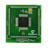
Manufacturer Part Number
MA180023
Description
MODULE PLUG-IN PIC18F46J11 PIM
Manufacturer
Microchip Technology
Series
PIC®r
Datasheet
1.MA180023.pdf
(528 pages)
Specifications of MA180023
Accessory Type
Plug-In Module (PIM) - PIC18F46J11
Tool / Board Applications
General Purpose MCU, MPU, DSP, DSC
Mcu Supported Families
PIC18
Supported Devices
Stand-alone Or W/ HPC(DM183022) Or PIC18(DM183032)
Silicon Manufacturer
Microchip
Core Architecture
PIC
Core Sub-architecture
PIC18
Silicon Core Number
PIC18F
Silicon Family Name
PIC18FxxJxx
Lead Free Status / RoHS Status
Lead free / RoHS Compliant
For Use With/related Products
HPC Explorer Board (DM183022) or PIC18 Explorer Board (DM183032)
For Use With
DM183032 - BOARD EXPLORER PICDEM PIC18DM183022 - BOARD DEMO PIC18FXX22 64/80TQFP
Lead Free Status / RoHS Status
Lead free / RoHS Compliant
Available stocks
Company
Part Number
Manufacturer
Quantity
Price
Company:

Part Number:
MA180023
Manufacturer:
Microchip Technology
Quantity:
135


4.2
The Master Clear Reset (MCLR) pin provides a method
for triggering a hard external Reset of the device. A
Reset is generated by holding the pin low. PIC18
extended microcontroller devices have a noise filter in
the MCLR Reset path, which detects and ignores small
pulses.
The MCLR pin is not driven low by any internal Resets,
including the WDT.
4.3
A POR condition is generated on-chip whenever V
rises above a certain threshold. This allows the device
to start in the initialized state when V
operation.
To take advantage of the POR circuitry, tie the MCLR
pin through a resistor (1 kΩ to 10 kΩ) to V
eliminate external RC components usually needed to
create a POR delay.
When the device starts normal operation (i.e., exits the
Reset
(voltage, frequency, temperature, etc.) must be met to
ensure operation. If these conditions are not met, the
device must be held in Reset until the operating
conditions are met.
POR events are captured by the POR bit (RCON<1>).
The state of the bit is set to ‘0’ whenever a Power-on
Reset occurs; it does not change for any other Reset
event. POR is not reset to ‘1’ by any hardware event.
To capture multiple events, the user manually resets
the bit to ‘1’ in software following any POR.
4.4
“F” devices incorporate two types of BOR circuits: one
which monitors V
Only one BOR circuit can be active at a time. When in
normal Run mode, Idle or normal Sleep modes, the
BOR circuit that monitors V
cause the device to be held in BOR if V
below V
back above V
the expiration of the Power-up Timer, with period,
T
During Deep Sleep operation, the on-chip core voltage
regulator is disabled and V
ground levels. If the Deep Sleep BOR circuit is enabled
by the DSBOREN Configuration bit (CONFIG3L<2> = 1),
it will monitor V
threshold, the device will be held in a Reset state
similar to POR. All registers will be set back to their POR
Reset values and the contents of the DSGPR0 and
DSGPR1 holding registers will be lost.
© 2009 Microchip Technology Inc.
PWRT
(parameter 33).
BOR
condition),
Master Clear (MCLR)
Power-on Reset (POR)
Brown-out Reset (BOR)
(parameter D005). Once V
BOR
DD
DDCORE
, the device will be held in Reset until
. If V
device
DD
and one which monitors V
DDCORE
drops below the V
DDCORE
operating
is allowed to drop to
DD
is active and will
is adequate for
DDCORE
DDCORE
DD
parameters
. This will
DSBOR
drops
rises
DD
DD
.
PIC18F46J11 FAMILY
Additionally, if any I/O pins had been configured as out-
puts during Deep Sleep, these pins will be tri-stated
and the device will no longer be held in Deep Sleep.
Once the V
V
achieves a V
will begin executing code again normally, but the DS bit
in the WDTCON register will not be set. The device
behavior will be similar to hard cycling all power to the
device.
On “LF” devices, the V
disabled because the internal core voltage regulator is
disabled. Instead of monitoring V
devices in this family can use the V
monitor V
The V
DSBOREN bit = 0.
The V
on “LF” devices, or on “F” devices while in Deep Sleep
with DSBOREN = 1. When enabled, the V
circuit is extremely low power (typ. 200 nA) during nor-
mal operation above ~2.3V on V
this DSBOR arming level when the V
enabled, the device may begin to consume additional
current (typ. 50 μA) as internal features of the circuit
power up. The higher current is necessary to achieve
more accurate sensing of the V
device will not enter Reset until V
V
4.4.1
The BOR bit always resets to ‘0’ on any V
or POR event. This makes it difficult to determine if a
Brown-out Reset event has occurred just by reading
the state of BOR alone. A more reliable method is to
simultaneously check the state of both POR and BOR.
This assumes that the POR bit is reset to ‘1’ in software
immediately after any Power-on Reset event. If BOR is
‘0’ while POR is ‘1’, it can be reliably assumed that a
Brown-out Reset event has occurred.
If the voltage regulator is disabled (LF devices), the
V
the BOR bit cannot be used to determine a Brown-out
Reset event. The BOR bit is still cleared by a Power-on
Reset event.
DSBOR
DSBOR
DDCORE
DD
DD
threshold, and once the core voltage regulator
threshold.
BOR circuit is enabled when DSBOREN = 1
DD
BOR circuit can be disabled by setting the
BOR functionality is disabled. In this case,
DETECTING BOR
DD
DDCORE
excursions below the V
voltage recovers back above the
voltage above V
DDCORE
DD
DD
BOR circuit is always
. If V
level. However, the
DDCORE
DD
DS39932C-page 59
DD
DSBOR
DD
BOR
DD
falls below the
BOR circuit to
DDCORE
BOR circuit is
drops below
, the device
, PIC18LF
threshold.
DD
, BOR
BOR
Related parts for MA180023
Image
Part Number
Description
Manufacturer
Datasheet
Request
R

Part Number:
Description:
Manufacturer:
Microchip Technology Inc.
Datasheet:
Part Number:
Description:
Manufacturer:
Microchip Technology Inc.
Datasheet:
Part Number:
Description:
Manufacturer:
Microchip Technology Inc.
Datasheet:
Part Number:
Description:
Manufacturer:
Microchip Technology Inc.
Datasheet:
Part Number:
Description:
Manufacturer:
Microchip Technology Inc.
Datasheet:
Part Number:
Description:
Manufacturer:
Microchip Technology Inc.
Datasheet:
Part Number:
Description:
Manufacturer:
Microchip Technology Inc.
Datasheet:
Part Number:
Description:
Manufacturer:
Microchip Technology Inc.
Datasheet: