MA180023 Microchip Technology, MA180023 Datasheet - Page 269
MA180023
Manufacturer Part Number
MA180023
Description
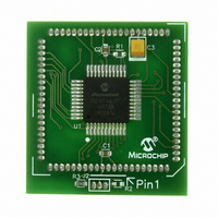
MODULE PLUG-IN PIC18F46J11 PIM
Manufacturer
Microchip Technology
Series
PIC®r
Datasheet
1.MA180023.pdf
(528 pages)
Specifications of MA180023
Accessory Type
Plug-In Module (PIM) - PIC18F46J11
Tool / Board Applications
General Purpose MCU, MPU, DSP, DSC
Mcu Supported Families
PIC18
Supported Devices
Stand-alone Or W/ HPC(DM183022) Or PIC18(DM183032)
Silicon Manufacturer
Microchip
Core Architecture
PIC
Core Sub-architecture
PIC18
Silicon Core Number
PIC18F
Silicon Family Name
PIC18FxxJxx
Lead Free Status / RoHS Status
Lead free / RoHS Compliant
For Use With/related Products
HPC Explorer Board (DM183022) or PIC18 Explorer Board (DM183032)
For Use With
DM183032 - BOARD EXPLORER PICDEM PIC18DM183022 - BOARD DEMO PIC18FXX22 64/80TQFP
Lead Free Status / RoHS Status
Lead free / RoHS Compliant
Available stocks
Company
Part Number
Manufacturer
Quantity
Price
Company:

Part Number:
MA180023
Manufacturer:
Microchip Technology
Quantity:
135


18.3.2
When initializing the SPI, several options need to be
specified. This is done by programming the appropriate
control bits (SSPxCON1<5:0> and SSPxSTAT<7:6>).
These control bits allow the following to be specified:
• Master mode (SCKx is the clock output)
• Slave mode (SCKx is the clock input)
• Clock Polarity (Idle state of SCKx)
• Data Input Sample Phase (middle or end of data
• Clock Edge (output data on rising/falling edge of
• Clock Rate (Master mode only)
• Slave Select mode (Slave mode only)
Each MSSP module consists of a transmit/receive shift
register (SSPxSR) and a buffer register (SSPxBUF).
The SSPxSR shifts the data in and out of the device,
MSb first. The SSPxBUF holds the data that was written
to the SSPxSR until the received data is ready. Once the
8 bits of data have been received, that byte is moved to
the SSPxBUF register. Then, the Buffer Full (BF) detect
bit (SSPxSTAT<0>) and the interrupt flag bit, SSPxIF,
are set. This double-buffering of the received data
(SSPxBUF) allows the next byte to start reception before
reading the data that was just received.
Any write to the SSPxBUF register during transmis-
sion/reception of data will be ignored and the Write
Collision Detect bit, WCOL (SSPxCON1<7>), will be set.
User software must clear the WCOL bit so that it can be
determined if the following write(s) to the SSPxBUF
register completed successfully.
EXAMPLE 18-1:
© 2009 Microchip Technology Inc.
LOOP
output time)
SCKx)
Note:
BTFSS
BRA
MOVF
MOVWF
MOVF
MOVWF
OPERATION
When the application software is expecting
to receive valid data, the SSPxBUF should
be read before the next byte of transfer
data is written to the SSPxBUF. Application
software should follow this process even
when the current contents of SSPxBUF
are not important.
SSP1STAT, BF
LOOP
SSP1BUF, W
RXDATA
TXDATA, W
SSP1BUF
LOADING THE SSP1BUF (SSP1SR) REGISTER
;Has data been received (transmit complete)?
;No
;WREG reg = contents of SSP1BUF
;Save in user RAM, if data is meaningful
;W reg = contents of TXDATA
;New data to xmit
PIC18F46J11 FAMILY
The Buffer Full bit, BF (SSPxSTAT<0>), indicates when
SSPxBUF has been loaded with the received data
(transmission is complete). When the SSPxBUF is read,
the BF bit is cleared. This data may be irrelevant if the
SPI is only a transmitter. Generally, the MSSP interrupt
is used to determine when the transmission/reception
has completed. If the interrupt method is not going to be
used, then software polling can be done to ensure that a
write collision does not occur.
Example 18-1 provides the loading of the SSPxBUF
(SSPxSR) for data transmission.
The SSPxSR is not directly readable or writable and
can only be accessed by addressing the SSPxBUF
register. Additionally, the SSPxSTAT register indicates
the various status conditions.
18.3.3
The drivers for the SDOx output and SCKx clock pins
can be optionally configured as open-drain outputs.
This feature allows the voltage level on the pin to be
pulled to a higher level through an external pull-up
resistor, provided the SDOx or SCKx pin is not multi-
plexed with an ANx analog function. This allows the
output to communicate with external circuits without the
need for additional level shifters. For more information,
see Section 9.1.4 “Open-Drain Outputs”.
The open-drain output option is controlled by the
SPI2OD and SPI1OD bits (ODCON3<1:0>). Setting an
SPIxOD bit configures both SDOx and SCKx pins for the
corresponding open-drain operation.
OPEN-DRAIN OUTPUT OPTION
DS39932C-page 269
Related parts for MA180023
Image
Part Number
Description
Manufacturer
Datasheet
Request
R

Part Number:
Description:
Manufacturer:
Microchip Technology Inc.
Datasheet:
Part Number:
Description:
Manufacturer:
Microchip Technology Inc.
Datasheet:
Part Number:
Description:
Manufacturer:
Microchip Technology Inc.
Datasheet:
Part Number:
Description:
Manufacturer:
Microchip Technology Inc.
Datasheet:
Part Number:
Description:
Manufacturer:
Microchip Technology Inc.
Datasheet:
Part Number:
Description:
Manufacturer:
Microchip Technology Inc.
Datasheet:
Part Number:
Description:
Manufacturer:
Microchip Technology Inc.
Datasheet:
Part Number:
Description:
Manufacturer:
Microchip Technology Inc.
Datasheet: