MA180023 Microchip Technology, MA180023 Datasheet - Page 278
MA180023
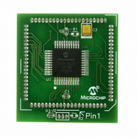
Manufacturer Part Number
MA180023
Description
MODULE PLUG-IN PIC18F46J11 PIM
Manufacturer
Microchip Technology
Series
PIC®r
Datasheet
1.MA180023.pdf
(528 pages)
Specifications of MA180023
Accessory Type
Plug-In Module (PIM) - PIC18F46J11
Tool / Board Applications
General Purpose MCU, MPU, DSP, DSC
Mcu Supported Families
PIC18
Supported Devices
Stand-alone Or W/ HPC(DM183022) Or PIC18(DM183032)
Silicon Manufacturer
Microchip
Core Architecture
PIC
Core Sub-architecture
PIC18
Silicon Core Number
PIC18F
Silicon Family Name
PIC18FxxJxx
Lead Free Status / RoHS Status
Lead free / RoHS Compliant
For Use With/related Products
HPC Explorer Board (DM183022) or PIC18 Explorer Board (DM183032)
For Use With
DM183032 - BOARD EXPLORER PICDEM PIC18DM183022 - BOARD DEMO PIC18FXX22 64/80TQFP
Lead Free Status / RoHS Status
Lead free / RoHS Compliant
Available stocks
Company
Part Number
Manufacturer
Quantity
Price
Company:

Part Number:
MA180023
Manufacturer:
Microchip Technology
Quantity:
135


PIC18F46J11 FAMILY
REGISTER 18-3:
DS39932C-page 278
bit 7
Legend:
R = Readable bit
-n = Value at POR
bit 7-6
bit 5
bit 4
bit 3-2
bit 1
bit 0
SSCON1
R/W-0
SSCON<1:0>: SSDMA Output Control bits (Master modes only)
11 = SSDMA is asserted for the duration of 4 bytes; DLYINTEN is always reset low
01 = SSDMA is asserted for the duration of 2 bytes; DLYINTEN is always reset low
10 = SSDMA is asserted for the duration of 1 byte; DLYINTEN is always reset low
00 = SSDMA is not controlled by the DMA module; DLYINTEN bit is software programmable
TXINC: Transmit Address Increment Enable bit
Allows the transmit address to increment as the transfer progresses.
1 = The transmit address is to be incremented from the initial value of TXADDR<11:0>
0 = The transmit address is always set to the initial value of TXADDR<11:0>
RXINC: Receive Address Increment Enable bit
Allows the receive address to increment as the transfer progresses.
1 = The received address is to be incremented from the intial value of RXADDR<11:0>
0 = The received address is always set to the initial value of RXADDR<11:0>
DUPLEX<1:0>: Transmit/Receive Operating Mode Select bits
10 = SPI DMA operates in Full-Duplex mode, data is simultaneously transmitted and received
01 = DMA operates in Half-Duplex mode, data is transmitted only
00 = DMA operates in Half-Duplex mode, data is received only
DLYINTEN: Delay Interrupt Enable bit
Enables the interrupt to be invoked after the number of SCK cycles specified in DLYCYC<2:0> has
elapsed from the latest completed transfer.
1 = The interrupt is enabled, SSCON<1:0> must be set to ‘00’
0 = The interrupt is disabled
DMAEN: DMA Operation Start/Stop bit
This bit is set by the users’ software to start the DMA operation. It is reset back to zero by the DMA
engine when the DMA operation is completed or aborted.
1 = DMA is in session
0 = DMA is not in session
SSCON0
R/W-0
DMACON1: DMA CONTROL REGISTER 1 (ACCESS F88h)
W = Writable bit
‘1’ = Bit is set
TXINC
R/W-0
RXINC
R/W-0
U = Unimplemented bit, read as ‘0’
‘0’ = Bit is cleared
DUPLEX1
R/W-0
DUPLEX0
R/W-0
© 2009 Microchip Technology Inc.
x = Bit is unknown
DLYINTEN
R/W-0
DMAEN
R/W-0
bit 0
Related parts for MA180023
Image
Part Number
Description
Manufacturer
Datasheet
Request
R

Part Number:
Description:
Manufacturer:
Microchip Technology Inc.
Datasheet:
Part Number:
Description:
Manufacturer:
Microchip Technology Inc.
Datasheet:
Part Number:
Description:
Manufacturer:
Microchip Technology Inc.
Datasheet:
Part Number:
Description:
Manufacturer:
Microchip Technology Inc.
Datasheet:
Part Number:
Description:
Manufacturer:
Microchip Technology Inc.
Datasheet:
Part Number:
Description:
Manufacturer:
Microchip Technology Inc.
Datasheet:
Part Number:
Description:
Manufacturer:
Microchip Technology Inc.
Datasheet:
Part Number:
Description:
Manufacturer:
Microchip Technology Inc.
Datasheet: