MA180023 Microchip Technology, MA180023 Datasheet - Page 293
MA180023
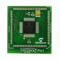
Manufacturer Part Number
MA180023
Description
MODULE PLUG-IN PIC18F46J11 PIM
Manufacturer
Microchip Technology
Series
PIC®r
Datasheet
1.MA180023.pdf
(528 pages)
Specifications of MA180023
Accessory Type
Plug-In Module (PIM) - PIC18F46J11
Tool / Board Applications
General Purpose MCU, MPU, DSP, DSC
Mcu Supported Families
PIC18
Supported Devices
Stand-alone Or W/ HPC(DM183022) Or PIC18(DM183032)
Silicon Manufacturer
Microchip
Core Architecture
PIC
Core Sub-architecture
PIC18
Silicon Core Number
PIC18F
Silicon Family Name
PIC18FxxJxx
Lead Free Status / RoHS Status
Lead free / RoHS Compliant
For Use With/related Products
HPC Explorer Board (DM183022) or PIC18 Explorer Board (DM183032)
For Use With
DM183032 - BOARD EXPLORER PICDEM PIC18DM183022 - BOARD DEMO PIC18FXX22 64/80TQFP
Lead Free Status / RoHS Status
Lead free / RoHS Compliant
Available stocks
Company
Part Number
Manufacturer
Quantity
Price
Company:

Part Number:
MA180023
Manufacturer:
Microchip Technology
Quantity:
135


18.5.3.5
When the R/W bit of the address byte is clear and an
address match occurs, the R/W bit of the SSPxSTAT
register is cleared. The received address is loaded into
the SSPxBUF register and the SDAx line is held low
(ACK).
When the address byte overflow condition exists, then
the no Acknowledge (ACK) pulse is given. An overflow
condition is defined as either bit, BF (SSPxSTAT<0>),
is set or bit, SSPOV (SSPxCON1<6>), is set.
An MSSP interrupt is generated for each data transfer
byte. The interrupt flag bit, SSPxIF, must be cleared in
software. The SSPxSTAT register is used to determine
the status of the byte.
If SEN is enabled (SSPxCON2<0> = 1), SCLx will be
held low (clock stretch) following each data transfer.
The clock must be released by setting bit, CKP
(SSPxCON1<4>).
Stretching” for more details.
© 2009 Microchip Technology Inc.
Reception
See
Section 18.5.4
“Clock
PIC18F46J11 FAMILY
18.5.3.6
When the R/W bit of the incoming address byte is set
and an address match occurs, the R/W bit of the
SSPxSTAT register is set. The received address is
loaded into the SSPxBUF register. The ACK pulse will
be sent on the ninth bit and pin SCLx is held low regard-
less of SEN (see Section 18.5.4 “Clock Stretching”
for more details). By stretching the clock, the master
will be unable to assert another clock pulse until the
slave is done preparing the transmit data. The transmit
data must be loaded into the SSPxBUF register, which
also loads the SSPxSR register. Then, the SCLx pin
should
(SSPxCON1<4>). The eight data bits are shifted out on
the falling edge of the SCLx input. This ensures that the
SDAx signal is valid during the SCLx high time
(Figure 18-10).
The ACK pulse from the master-receiver is latched on
the rising edge of the ninth SCLx input pulse. If the
SDAx line is high (not ACK), then the data transfer is
complete. In this case, when the ACK is latched by the
slave, the slave logic is reset (resets the SSPxSTAT
register) and the slave monitors for another occurrence
of the Start bit. If the SDAx line was low (ACK), the next
transmit data must be loaded into the SSPxBUF
register. Again, the SCLx pin must be enabled by
setting bit, CKP.
An MSSP interrupt is generated for each data transfer
byte. The SSPxIF bit must be cleared in software and
the SSPxSTAT register is used to determine the status
of the byte. The SSPxIF bit is set on the falling edge of
the ninth clock pulse.
be
Transmission
enabled
by
setting
DS39932C-page 293
bit,
CKP
Related parts for MA180023
Image
Part Number
Description
Manufacturer
Datasheet
Request
R

Part Number:
Description:
Manufacturer:
Microchip Technology Inc.
Datasheet:
Part Number:
Description:
Manufacturer:
Microchip Technology Inc.
Datasheet:
Part Number:
Description:
Manufacturer:
Microchip Technology Inc.
Datasheet:
Part Number:
Description:
Manufacturer:
Microchip Technology Inc.
Datasheet:
Part Number:
Description:
Manufacturer:
Microchip Technology Inc.
Datasheet:
Part Number:
Description:
Manufacturer:
Microchip Technology Inc.
Datasheet:
Part Number:
Description:
Manufacturer:
Microchip Technology Inc.
Datasheet:
Part Number:
Description:
Manufacturer:
Microchip Technology Inc.
Datasheet: