MA180023 Microchip Technology, MA180023 Datasheet - Page 348
MA180023
Manufacturer Part Number
MA180023
Description
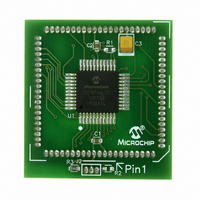
MODULE PLUG-IN PIC18F46J11 PIM
Manufacturer
Microchip Technology
Series
PIC®r
Datasheet
1.MA180023.pdf
(528 pages)
Specifications of MA180023
Accessory Type
Plug-In Module (PIM) - PIC18F46J11
Tool / Board Applications
General Purpose MCU, MPU, DSP, DSC
Mcu Supported Families
PIC18
Supported Devices
Stand-alone Or W/ HPC(DM183022) Or PIC18(DM183032)
Silicon Manufacturer
Microchip
Core Architecture
PIC
Core Sub-architecture
PIC18
Silicon Core Number
PIC18F
Silicon Family Name
PIC18FxxJxx
Lead Free Status / RoHS Status
Lead free / RoHS Compliant
For Use With/related Products
HPC Explorer Board (DM183022) or PIC18 Explorer Board (DM183032)
For Use With
DM183032 - BOARD EXPLORER PICDEM PIC18DM183022 - BOARD DEMO PIC18FXX22 64/80TQFP
Lead Free Status / RoHS Status
Lead free / RoHS Compliant
Available stocks
Company
Part Number
Manufacturer
Quantity
Price
Company:

Part Number:
MA180023
Manufacturer:
Microchip Technology
Quantity:
135


PIC18F46J11 FAMILY
The analog reference voltage is software select-
able to either the device’s positive and negative
supply voltage (AV
level
RA2/AN2/V
The A/D Converter has a unique feature of being able
to operate while the device is in Sleep mode. To
operate in Sleep, the A/D conversion clock must be
derived from the A/D’s internal RC oscillator.
The output of the sample and hold is the input into the
Converter, which generates the result via successive
approximation.
FIGURE 20-1:
DS39932C-page 348
Note 1: Channels AN5, AN6 and AN7 are not available on 28-pin devices.
on
REF
Converter
2: I/O pins have diode protection to V
the
-/CV
10-Bit
A/D
Reference
REF
DD
Voltage
RA3/AN3/V
A/D BLOCK DIAGRAM
/C2INB pins.
and AV
SS
REF
), or the voltage
V
+/C1INB
V
REF
REF
+
-
(Input Voltage)
VCFG<1:0>
V
DD
AIN
and
and V
SS
V
.
DD
V
(2)
SS (2)
Each port pin associated with the A/D Converter can be
configured as an analog input or as a digital I/O. The
ADRESH and ADRESL registers contain the result of
the A/D conversion. When the A/D conversion is com-
plete, the result is loaded into the ADRESH:ADRESL
register pair, the GO/DONE bit (ADCON0<1>) is
cleared and the A/D Interrupt Flag bit, ADIF, is set.
A device Reset forces all registers to their Reset state.
This forces the A/D module to be turned off and any
conversion in progress is aborted. The value in the
ADRESH:ADRESL register pair is not modified for a
Power-on Reset (POR). These registers will contain
unknown data after a POR.
Figure 20-1 provides the block diagram of the A/D module.
CHS<3:0>
1111
1110
1100
1011
1010
1001
1000
0111
0110
0101
0100
0011
0010
0001
0000
© 2009 Microchip Technology Inc.
V
V
AN12
AN11
AN10
AN9
AN8
AN7
AN6
AN5
AN4
AN3
AN2
AN1
AN0
BG
DDCORE
(1)
(1)
(1)
/V
CAP
Related parts for MA180023
Image
Part Number
Description
Manufacturer
Datasheet
Request
R

Part Number:
Description:
Manufacturer:
Microchip Technology Inc.
Datasheet:
Part Number:
Description:
Manufacturer:
Microchip Technology Inc.
Datasheet:
Part Number:
Description:
Manufacturer:
Microchip Technology Inc.
Datasheet:
Part Number:
Description:
Manufacturer:
Microchip Technology Inc.
Datasheet:
Part Number:
Description:
Manufacturer:
Microchip Technology Inc.
Datasheet:
Part Number:
Description:
Manufacturer:
Microchip Technology Inc.
Datasheet:
Part Number:
Description:
Manufacturer:
Microchip Technology Inc.
Datasheet:
Part Number:
Description:
Manufacturer:
Microchip Technology Inc.
Datasheet: