MA180023 Microchip Technology, MA180023 Datasheet - Page 439
MA180023
Manufacturer Part Number
MA180023
Description
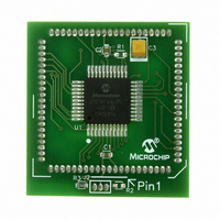
MODULE PLUG-IN PIC18F46J11 PIM
Manufacturer
Microchip Technology
Series
PIC®r
Datasheet
1.MA180023.pdf
(528 pages)
Specifications of MA180023
Accessory Type
Plug-In Module (PIM) - PIC18F46J11
Tool / Board Applications
General Purpose MCU, MPU, DSP, DSC
Mcu Supported Families
PIC18
Supported Devices
Stand-alone Or W/ HPC(DM183022) Or PIC18(DM183032)
Silicon Manufacturer
Microchip
Core Architecture
PIC
Core Sub-architecture
PIC18
Silicon Core Number
PIC18F
Silicon Family Name
PIC18FxxJxx
Lead Free Status / RoHS Status
Lead free / RoHS Compliant
For Use With/related Products
HPC Explorer Board (DM183022) or PIC18 Explorer Board (DM183032)
For Use With
DM183032 - BOARD EXPLORER PICDEM PIC18DM183022 - BOARD DEMO PIC18FXX22 64/80TQFP
Lead Free Status / RoHS Status
Lead free / RoHS Compliant
Available stocks
Company
Part Number
Manufacturer
Quantity
Price
Company:

Part Number:
MA180023
Manufacturer:
Microchip Technology
Quantity:
135


RETURN
Syntax:
Operands:
Operation:
Status Affected:
Encoding:
Description:
Words:
Cycles:
Example:
© 2009 Microchip Technology Inc.
Q Cycle Activity:
After Instruction:
operation
Decode
No
PC = TOS
Q1
operation
operation
Return from Subroutine
RETURN {s}
s ∈ [0,1]
(TOS) → PC;
if s = 1,
(WS) → W,
(STATUSS) → STATUS,
(BSRS) → BSR,
PCLATU, PCLATH are unchanged
None
Return from subroutine. The stack is
popped and the top of the stack (TOS)
is loaded into the program counter. If
‘s’= 1, the contents of the shadow
registers WS, STATUSS and BSRS are
loaded into their corresponding
registers W, STATUS and BSR. If
‘s’ = 0, no update of these registers
occurs (default).
1
2
RETURN
0000
No
No
Q2
0000
operation
Process
Data
No
Q3
0001
from stack
operation
POP PC
No
Q4
001s
PIC18F46J11 FAMILY
RLCF
Syntax:
Operands:
Operation:
Status Affected:
Encoding:
Description:
Words:
Cycles:
Example:
Q Cycle Activity:
Before Instruction
After Instruction
Decode
REG
C
REG
W
C
Q1
Rotate Left f through Carry
The contents of register ‘f’ are rotated
0 ≤ f ≤ 255
d ∈ [0,1]
a ∈ [0,1]
(f<n>) → dest<n + 1>,
(f<7>) → C,
(C) → dest<0>
C, N, Z
one bit to the left through the Carry flag.
If ‘d’ is ‘0’, the result is placed in W. If ‘d’
is ‘1’, the result is stored back in register
‘f’ (default).
If ‘a’ is ‘0’, the Access Bank is selected.
If ‘a’ is ‘1’, the BSR is used to select the
GPR bank (default).
If ‘a’ is ‘0’ and the extended instruction
set is enabled, this instruction operates
in Indexed Literal Offset Addressing
mode whenever f ≤ 95 (5Fh). See
Section 26.2.3 “Byte-Oriented and
Bit-Oriented Instructions in Indexed
Literal Offset Mode” for details.
1
1
register ‘f’
=
=
=
=
=
RLCF
Read
0011
RLCF
Q2
1110 0110
0
1110 0110
1100 1100
1
C
f {,d {,a}}
01da
Process
REG, 0, 0
Data
Q3
register f
DS39932C-page 439
ffff
destination
Write to
Q4
ffff
Related parts for MA180023
Image
Part Number
Description
Manufacturer
Datasheet
Request
R

Part Number:
Description:
Manufacturer:
Microchip Technology Inc.
Datasheet:
Part Number:
Description:
Manufacturer:
Microchip Technology Inc.
Datasheet:
Part Number:
Description:
Manufacturer:
Microchip Technology Inc.
Datasheet:
Part Number:
Description:
Manufacturer:
Microchip Technology Inc.
Datasheet:
Part Number:
Description:
Manufacturer:
Microchip Technology Inc.
Datasheet:
Part Number:
Description:
Manufacturer:
Microchip Technology Inc.
Datasheet:
Part Number:
Description:
Manufacturer:
Microchip Technology Inc.
Datasheet:
Part Number:
Description:
Manufacturer:
Microchip Technology Inc.
Datasheet: