MA180023 Microchip Technology, MA180023 Datasheet - Page 98
MA180023
Manufacturer Part Number
MA180023
Description
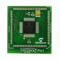
MODULE PLUG-IN PIC18F46J11 PIM
Manufacturer
Microchip Technology
Series
PIC®r
Datasheet
1.MA180023.pdf
(528 pages)
Specifications of MA180023
Accessory Type
Plug-In Module (PIM) - PIC18F46J11
Tool / Board Applications
General Purpose MCU, MPU, DSP, DSC
Mcu Supported Families
PIC18
Supported Devices
Stand-alone Or W/ HPC(DM183022) Or PIC18(DM183032)
Silicon Manufacturer
Microchip
Core Architecture
PIC
Core Sub-architecture
PIC18
Silicon Core Number
PIC18F
Silicon Family Name
PIC18FxxJxx
Lead Free Status / RoHS Status
Lead free / RoHS Compliant
For Use With/related Products
HPC Explorer Board (DM183022) or PIC18 Explorer Board (DM183032)
For Use With
DM183032 - BOARD EXPLORER PICDEM PIC18DM183022 - BOARD DEMO PIC18FXX22 64/80TQFP
Lead Free Status / RoHS Status
Lead free / RoHS Compliant
Available stocks
Company
Part Number
Manufacturer
Quantity
Price
Company:

Part Number:
MA180023
Manufacturer:
Microchip Technology
Quantity:
135


PIC18F46J11 FAMILY
FIGURE 6-2:
6.2
Several control registers are used in conjunction with
the TBLRD and TBLWT instructions. Those are:
• EECON1 register
• EECON2 register
• TABLAT register
• TBLPTR registers
6.2.1
The EECON1 register (Register 6-1) is the control
register for memory accesses. The EECON2 register is
not a physical register; it is used exclusively in the
memory
EECON2 will read all ‘0’s.
The WPROG bit, when set, will allow programming
two bytes per word on the execution of the WR
command. If this bit is cleared, the WR command will
result in programming on a block of 64 bytes.
DS39932C-page 98
Note 1:
Control Registers
write
TBLPTRU
EECON1 AND EECON2 REGISTERS
Table Pointer actually points to one of 64 holding registers, the address of which is determined by
TBLPTRL<5:0>. The process for physically writing data to the program memory array is discussed in
Section 6.5 “Writing to Flash Program Memory”.
and
Table Pointer
TBLPTRH
TABLE WRITE OPERATION
erase
(1)
sequences.
TBLPTRL
Program Memory
(TBLPTR)
Reading
Instruction: TBLWT*
Holding Registers
Program Memory
The FREE bit, when set, will allow a program memory
erase operation. When FREE is set, the erase
operation is initiated on the next WR command. When
FREE is clear, only writes are enabled.
The WREN bit, when set, will allow a write operation.
On power-up, the WREN bit is clear. The WRERR bit is
set in hardware when the WR bit is set, and cleared
when the internal programming timer expires and the
write operation is complete.
The WR control bit initiates write operations. The bit
cannot be cleared, only set, in software. It is cleared in
hardware at the completion of the write operation.
Note:
During normal operation, the WRERR is
read as ‘1’. This can indicate that a write
operation was prematurely terminated by
a Reset, or a write operation was
attempted improperly.
© 2009 Microchip Technology Inc.
Table Latch (8-bit)
TABLAT
Related parts for MA180023
Image
Part Number
Description
Manufacturer
Datasheet
Request
R

Part Number:
Description:
Manufacturer:
Microchip Technology Inc.
Datasheet:
Part Number:
Description:
Manufacturer:
Microchip Technology Inc.
Datasheet:
Part Number:
Description:
Manufacturer:
Microchip Technology Inc.
Datasheet:
Part Number:
Description:
Manufacturer:
Microchip Technology Inc.
Datasheet:
Part Number:
Description:
Manufacturer:
Microchip Technology Inc.
Datasheet:
Part Number:
Description:
Manufacturer:
Microchip Technology Inc.
Datasheet:
Part Number:
Description:
Manufacturer:
Microchip Technology Inc.
Datasheet:
Part Number:
Description:
Manufacturer:
Microchip Technology Inc.
Datasheet: