MA180023 Microchip Technology, MA180023 Datasheet - Page 283
MA180023
Manufacturer Part Number
MA180023
Description
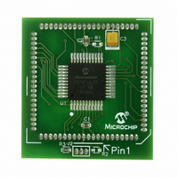
MODULE PLUG-IN PIC18F46J11 PIM
Manufacturer
Microchip Technology
Series
PIC®r
Datasheet
1.MA180023.pdf
(528 pages)
Specifications of MA180023
Accessory Type
Plug-In Module (PIM) - PIC18F46J11
Tool / Board Applications
General Purpose MCU, MPU, DSP, DSC
Mcu Supported Families
PIC18
Supported Devices
Stand-alone Or W/ HPC(DM183022) Or PIC18(DM183032)
Silicon Manufacturer
Microchip
Core Architecture
PIC
Core Sub-architecture
PIC18
Silicon Core Number
PIC18F
Silicon Family Name
PIC18FxxJxx
Lead Free Status / RoHS Status
Lead free / RoHS Compliant
For Use With/related Products
HPC Explorer Board (DM183022) or PIC18 Explorer Board (DM183032)
For Use With
DM183032 - BOARD EXPLORER PICDEM PIC18DM183022 - BOARD DEMO PIC18FXX22 64/80TQFP
Lead Free Status / RoHS Status
Lead free / RoHS Compliant
Available stocks
Company
Part Number
Manufacturer
Quantity
Price
Company:

Part Number:
MA180023
Manufacturer:
Microchip Technology
Quantity:
135


EXAMPLE 18-2:
© 2009 Microchip Technology Inc.
InitSPIPins:
InitMSSP2:
InitSPIDMA:
movwf
movlw
movwf
bsf
movlb
bcf
bcf
bcf
bcf
bcf
bsf
movlb
bcf
movlw
movwf
movlw
movwf
bcf
bsf
movlw
movwf
movlw
movwf
movlw
movlb
clrf
movlw
movwf
bsf
movlw
movwf
movlw
movwf
0x0F
ODCON3, SPI2OD
LATB, RB2
LATB, RB1
TRISB, RB1
TRISB, RB2
TRISB, RB0
0x0E
INTCON, GIE
0x55
EECON2
0xAA
EECON2
PPSCON, IOLOCK
INTCON, GIE
0x03
RPINR21
0x0A
RPOR4
0x04
RPINR22
0x09
RPOR5
PPSCON, IOLOCK
0x0F
SSP2STAT
b'00000000'
SSP2CON1
SSP2CON1, SSPEN
b'00111110'
DMACON1
b'11110000'
DMACON2
512-BYTE SPI MASTER MODE Init AND TRANSFER
;For this example, let's use RP5(RB2) for SCK2,
;RP4(RB1) for SDO2, and RP3(RB0) for SDI2
;Let’s use SPI master mode, CKE = 0, CKP = 0,
;without using slave select signalling.
;Select bank 15, for access to ODCON3 register
;Let’s not use open drain outputs in this example
;Initialize our (to be) SCK2 pin low (idle).
;Initialize our (to be) SDO2 pin to an idle state
;Make SDO2 output, and drive low
;Make SCK2 output, and drive low (idle state)
;SDI2 is an input, make sure it is tri-stated
;Now we should unlock the PPS registers, so we can
;assign the MSSP2 functions to our desired I/O pins.
;Select bank 14 for access to PPS registers
;I/O Pin unlock sequence will not work if CPU
;services an interrupt during the sequence
;Unlock sequence consists of writing 0x55
;and 0xAA to the EECON2 register.
;We may now write to RPINRx and RPORx registers
;May now turn back on interrupts if desired
;0x0A is SCK2 output signal
;Assign the SDI2 function to pin RP3
;Let’s assign SCK2 output to pin RP4
;RPOR4 maps output signals to RP4 pin
;SCK2 also needs to be configured as an input on the
;SCK2 input function taken from RP4 pin
;0x09 is SDO2 output
;Assign SDO2 output signal to the RP5 (RB2) pin
;Lock the PPS registers to prevent changes
;Done with PPS registers, bank 15 has other SFRs
;CKE = 0, SMP = 0 (sampled at middle of bit)
;CKP = 0, SPI Master mode, Fosc/4
;MSSP2 initialized
;Enable the MSSP2 module
;Full duplex, RX/TXINC enabled, no SSCON
;DLYINTEN is set, so DLYCYC3:DLYCYC0 = 1111
;Minimum delay between bytes, interrupt
;only once when the transaction is complete
same pin
PIC18F46J11 FAMILY
DS39932C-page 283
Related parts for MA180023
Image
Part Number
Description
Manufacturer
Datasheet
Request
R

Part Number:
Description:
Manufacturer:
Microchip Technology Inc.
Datasheet:
Part Number:
Description:
Manufacturer:
Microchip Technology Inc.
Datasheet:
Part Number:
Description:
Manufacturer:
Microchip Technology Inc.
Datasheet:
Part Number:
Description:
Manufacturer:
Microchip Technology Inc.
Datasheet:
Part Number:
Description:
Manufacturer:
Microchip Technology Inc.
Datasheet:
Part Number:
Description:
Manufacturer:
Microchip Technology Inc.
Datasheet:
Part Number:
Description:
Manufacturer:
Microchip Technology Inc.
Datasheet:
Part Number:
Description:
Manufacturer:
Microchip Technology Inc.
Datasheet: