MA180023 Microchip Technology, MA180023 Datasheet - Page 126
MA180023
Manufacturer Part Number
MA180023
Description
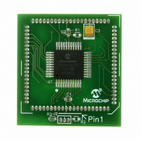
MODULE PLUG-IN PIC18F46J11 PIM
Manufacturer
Microchip Technology
Series
PIC®r
Datasheet
1.MA180023.pdf
(528 pages)
Specifications of MA180023
Accessory Type
Plug-In Module (PIM) - PIC18F46J11
Tool / Board Applications
General Purpose MCU, MPU, DSP, DSC
Mcu Supported Families
PIC18
Supported Devices
Stand-alone Or W/ HPC(DM183022) Or PIC18(DM183032)
Silicon Manufacturer
Microchip
Core Architecture
PIC
Core Sub-architecture
PIC18
Silicon Core Number
PIC18F
Silicon Family Name
PIC18FxxJxx
Lead Free Status / RoHS Status
Lead free / RoHS Compliant
For Use With/related Products
HPC Explorer Board (DM183022) or PIC18 Explorer Board (DM183032)
For Use With
DM183032 - BOARD EXPLORER PICDEM PIC18DM183022 - BOARD DEMO PIC18FXX22 64/80TQFP
Lead Free Status / RoHS Status
Lead free / RoHS Compliant
Available stocks
Company
Part Number
Manufacturer
Quantity
Price
Company:

Part Number:
MA180023
Manufacturer:
Microchip Technology
Quantity:
135


PIC18F46J11 FAMILY
9.1.3
Though the V
these devices are still capable of interfacing with 5V
systems, even if the V
3.6V. This is accomplished by adding a pull-up resistor
to the port pin (Figure 9-2), clearing the LAT bit for that
pin and manipulating the corresponding TRIS bit
(Figure 9-1) to either allow the line to be pulled high or
to drive the pin low. Only port pins that are tolerant of
voltages up to 5.5V can be used for this type of
interface (refer to Section 9.1.2 “Input Pins and
Voltage Considerations”).
FIGURE 9-2:
EXAMPLE 9-1:
9.1.4
The output pins for several peripherals are also
equipped with a configurable open-drain output option.
This allows the peripherals to communicate with
external digital logic operating at a higher voltage level,
without the use of level translators.
DS39932C-page 126
BCF
BCF
BCF
PIC18F46J11
LATD, 7
TRISD, 7 ; send a 0 to the 5V system
TRISD, 7 ; send a 1 to the 5V system
INTERFACING TO A 5V SYSTEM
OPEN-DRAIN OUTPUTS
RD7
DDMAX
; set up LAT register so
; changing TRIS bit will
; drive line low
of the PIC18F46J11 family is 3.6V,
IH
+5V SYSTEM HARDWARE
INTERFACE
COMMUNICATING WITH
THE +5V SYSTEM
of the target system is above
+5V
+5V Device
The open-drain option is implemented on port pins
specifically associated with the data and clock outputs
of the EUSARTs, the MSSP modules (in SPI mode) and
the ECCP modules. It is selectively enabled by setting
the open-drain control bit for the corresponding module
in the ODCON registers (Register 9-1, Register 9-2
and Register 9-3). Their configuration is discussed in
more detail with the individual port where these
peripherals are multiplexed.
When the open-drain option is required, the output pin
must also be tied through an external pull-up resistor
provided by the user to a higher voltage level, up to
5.5V (Figure 9-3). When a digital logic high signal is
output, it is pulled up to the higher voltage level.
FIGURE 9-3:
9.1.5
Many of the digital I/O ports use Schmitt Trigger (ST)
input buffers. While this form of buffering works well
with many types of input, some applications may
require TTL level signals to interface with external logic
devices. This is particularly true for the Parallel Master
Port (PMP), which is likely to be interfaced to TTL level
logic or memory devices.
The inputs for the PMP can be optionally configured for
TTL buffers with the PMPTTL bit in the PADCFG1 reg-
ister (Register 9-4). Setting this bit configures all data
and control input pins for the PMP to use TTL buffers.
By default, these PMP inputs use the port’s ST buffers.
3.3V
TTL INPUT BUFFER OPTION
V
DD
PIC18F46J11
(at logic ‘1’)
USING THE OPEN-DRAIN
OUTPUT (USART SHOWN
AS EXAMPLE)
© 2009 Microchip Technology Inc.
TX
X
+5V
5V
Related parts for MA180023
Image
Part Number
Description
Manufacturer
Datasheet
Request
R

Part Number:
Description:
Manufacturer:
Microchip Technology Inc.
Datasheet:
Part Number:
Description:
Manufacturer:
Microchip Technology Inc.
Datasheet:
Part Number:
Description:
Manufacturer:
Microchip Technology Inc.
Datasheet:
Part Number:
Description:
Manufacturer:
Microchip Technology Inc.
Datasheet:
Part Number:
Description:
Manufacturer:
Microchip Technology Inc.
Datasheet:
Part Number:
Description:
Manufacturer:
Microchip Technology Inc.
Datasheet:
Part Number:
Description:
Manufacturer:
Microchip Technology Inc.
Datasheet:
Part Number:
Description:
Manufacturer:
Microchip Technology Inc.
Datasheet: