MA180023 Microchip Technology, MA180023 Datasheet - Page 271
MA180023
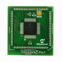
Manufacturer Part Number
MA180023
Description
MODULE PLUG-IN PIC18F46J11 PIM
Manufacturer
Microchip Technology
Series
PIC®r
Datasheet
1.MA180023.pdf
(528 pages)
Specifications of MA180023
Accessory Type
Plug-In Module (PIM) - PIC18F46J11
Tool / Board Applications
General Purpose MCU, MPU, DSP, DSC
Mcu Supported Families
PIC18
Supported Devices
Stand-alone Or W/ HPC(DM183022) Or PIC18(DM183032)
Silicon Manufacturer
Microchip
Core Architecture
PIC
Core Sub-architecture
PIC18
Silicon Core Number
PIC18F
Silicon Family Name
PIC18FxxJxx
Lead Free Status / RoHS Status
Lead free / RoHS Compliant
For Use With/related Products
HPC Explorer Board (DM183022) or PIC18 Explorer Board (DM183032)
For Use With
DM183032 - BOARD EXPLORER PICDEM PIC18DM183022 - BOARD DEMO PIC18FXX22 64/80TQFP
Lead Free Status / RoHS Status
Lead free / RoHS Compliant
Available stocks
Company
Part Number
Manufacturer
Quantity
Price
Company:

Part Number:
MA180023
Manufacturer:
Microchip Technology
Quantity:
135


18.3.6
The master can initiate the data transfer at any time
because it controls the SCKx. The master determines
when the slave (Processor 2, Figure 18-2) is to
broadcast data by the software protocol.
In Master mode, the data is transmitted/received as
soon as the SSPxBUF register is written to. If the SPI
is only going to receive, the SDOx output could be dis-
abled (programmed as an input). The SSPxSR register
will continue to shift in the signal present on the SDIx
pin at the programmed clock rate. As each byte is
received, it will be loaded into the SSPxBUF register as
if a normal received byte (interrupts and status bits
appropriately set). This could be useful in receiver
applications as a “Line Activity Monitor” mode.
The CKP is selected by appropriately programming the
CKP bit (SSPxCON1<4>). This then, would give
waveforms for SPI communication as illustrated in
Figure 18-3, Figure 18-5 and Figure 18-6, where the
FIGURE 18-3:
© 2009 Microchip Technology Inc.
Write to
SSPxBUF
SCKx
(CKP = 0
CKE = 0)
SCKx
(CKP = 1
CKE = 0)
SCKx
(CKP = 0
CKE = 1)
SCKx
(CKP = 1
CKE = 1)
SDOx
(CKE = 0)
SDOx
(CKE = 1)
SDIx
(SMP = 0)
Input
Sample
(SMP = 0)
SDIx
(SMP = 1)
Input
Sample
(SMP = 1)
SSPxIF
SSPxSR to
SSPxBUF
MASTER MODE
SPI MODE WAVEFORM (MASTER MODE)
bit 7
bit 7
bit 7
bit 7
bit 6
bit 6
bit 5
bit 5
bit 4
bit 4
PIC18F46J11 FAMILY
bit 3
bit 3
Most Significant Byte (MSB) is transmitted first. In
Master mode, the SPI clock rate (bit rate) is
user-programmable to be one of the following:
• F
• F
• F
• Timer2 output/2
When using the Timer2 output/2 option, the Period
Register 2 (PR2) can be used to determine the SPI bit
rate. However, only PR2 values of 0x01 to 0xFF are
valid in this mode.
Figure 18-3 illustrates the waveforms for Master mode.
When the CKE bit is set, the SDOx data is valid before
there is a clock edge on SCKx. The change of the input
sample is shown based on the state of the SMP bit. The
time when the SSPxBUF is loaded with the received
data is shown.
OSC
OSC
OSC
/4 (or T
/16 (or 4 • T
/64 (or 16 • T
bit 2
bit 2
CY
)
bit 1
bit 1
CY
CY
)
)
bit 0
bit 0
bit 0
bit 0
DS39932C-page 271
Next Q4 Cycle
after Q2↓
4 Clock
Modes
Related parts for MA180023
Image
Part Number
Description
Manufacturer
Datasheet
Request
R

Part Number:
Description:
Manufacturer:
Microchip Technology Inc.
Datasheet:
Part Number:
Description:
Manufacturer:
Microchip Technology Inc.
Datasheet:
Part Number:
Description:
Manufacturer:
Microchip Technology Inc.
Datasheet:
Part Number:
Description:
Manufacturer:
Microchip Technology Inc.
Datasheet:
Part Number:
Description:
Manufacturer:
Microchip Technology Inc.
Datasheet:
Part Number:
Description:
Manufacturer:
Microchip Technology Inc.
Datasheet:
Part Number:
Description:
Manufacturer:
Microchip Technology Inc.
Datasheet:
Part Number:
Description:
Manufacturer:
Microchip Technology Inc.
Datasheet: