MA180023 Microchip Technology, MA180023 Datasheet - Page 252
MA180023
Manufacturer Part Number
MA180023
Description
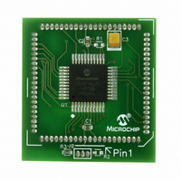
MODULE PLUG-IN PIC18F46J11 PIM
Manufacturer
Microchip Technology
Series
PIC®r
Datasheet
1.MA180023.pdf
(528 pages)
Specifications of MA180023
Accessory Type
Plug-In Module (PIM) - PIC18F46J11
Tool / Board Applications
General Purpose MCU, MPU, DSP, DSC
Mcu Supported Families
PIC18
Supported Devices
Stand-alone Or W/ HPC(DM183022) Or PIC18(DM183032)
Silicon Manufacturer
Microchip
Core Architecture
PIC
Core Sub-architecture
PIC18
Silicon Core Number
PIC18F
Silicon Family Name
PIC18FxxJxx
Lead Free Status / RoHS Status
Lead free / RoHS Compliant
For Use With/related Products
HPC Explorer Board (DM183022) or PIC18 Explorer Board (DM183032)
For Use With
DM183032 - BOARD EXPLORER PICDEM PIC18DM183022 - BOARD DEMO PIC18FXX22 64/80TQFP
Lead Free Status / RoHS Status
Lead free / RoHS Compliant
Available stocks
Company
Part Number
Manufacturer
Quantity
Price
Company:

Part Number:
MA180023
Manufacturer:
Microchip Technology
Quantity:
135


PIC18F46J11 FAMILY
17.5.1
In Half-Bridge mode, two pins are used as outputs to
drive push-pull loads. The PWM output signal is output
on the PxA pin, while the complementary PWM output
signal is output on the PxB pin (see Figure 17-8). This
mode can be used for half-bridge applications, as
shown in Figure 17-9, or for full-bridge applications,
where four power switches are being modulated with
two PWM signals.
In Half-Bridge mode, the programmable dead-band delay
can be used to prevent shoot-through current in
half-bridge power devices. The value of the PxDC<6:0>
bits of the ECCPxDEL register sets the number of
instruction cycles before the output is driven active. If the
value is greater than the duty cycle, the corresponding
output remains inactive during the entire cycle. See
Section 17.5.6 “Programmable Dead-Band Delay
Mode” for more details of the dead-band delay
operations.
FIGURE 17-9:
DS39932C-page 252
Standard Half-Bridge Circuit (“Push-Pull”)
Half-Bridge Output Driving a Full-Bridge Circuit
HALF-BRIDGE MODE
EXAMPLE OF HALF-BRIDGE APPLICATIONS
PxA
PxB
PxA
PxB
FET
Driver
FET
Driver
FET
Driver
FET
Driver
Since the PxA and PxB outputs are multiplexed with the
PORT data latches, the associated TRIS bits must be
cleared to configure PxA and PxB as outputs.
FIGURE 17-8:
PxA
PxB
td = Dead-Band Delay
Note 1: At this time, the TMR2 register is equal to the
(2)
(2)
2: Output signals are shown as active-high.
(1)
Load
V+
td
PR2 register.
Pulse Width
Period
Load
td
EXAMPLE OF
HALF-BRIDGE PWM
OUTPUT
© 2009 Microchip Technology Inc.
FET
Driver
FET
Driver
(1)
+
-
+
-
Period
(1)
Related parts for MA180023
Image
Part Number
Description
Manufacturer
Datasheet
Request
R

Part Number:
Description:
Manufacturer:
Microchip Technology Inc.
Datasheet:
Part Number:
Description:
Manufacturer:
Microchip Technology Inc.
Datasheet:
Part Number:
Description:
Manufacturer:
Microchip Technology Inc.
Datasheet:
Part Number:
Description:
Manufacturer:
Microchip Technology Inc.
Datasheet:
Part Number:
Description:
Manufacturer:
Microchip Technology Inc.
Datasheet:
Part Number:
Description:
Manufacturer:
Microchip Technology Inc.
Datasheet:
Part Number:
Description:
Manufacturer:
Microchip Technology Inc.
Datasheet:
Part Number:
Description:
Manufacturer:
Microchip Technology Inc.
Datasheet: