C8051F560-TB Silicon Laboratories Inc, C8051F560-TB Datasheet - Page 16
C8051F560-TB
Manufacturer Part Number
C8051F560-TB
Description
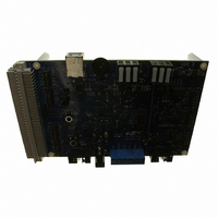
BOARD PROTOTYPE W/C8051F560
Manufacturer
Silicon Laboratories Inc
Type
MCUr
Datasheet
1.TOOLSTICK560DC.pdf
(302 pages)
Specifications of C8051F560-TB
Contents
Board
Processor To Be Evaluated
C8051F56x
Processor Series
C8051F56x
Interface Type
USB
Maximum Operating Temperature
+ 125 C
Minimum Operating Temperature
- 40 C
Operating Supply Voltage
1.8 V to 5.25 V
Lead Free Status / RoHS Status
Lead free / RoHS Compliant
For Use With/related Products
C8051F55x, C8051F56x, C8051F57x
For Use With
336-1691 - KIT DEVELOPMENT FOR C8051F560
Lead Free Status / Rohs Status
Lead free / RoHS Compliant
Other names
336-1694


C8051F55x/56x/57x
1. System Overview
C8051F55x/56x/57x devices are fully integrated mixed-signal System-on-a-Chip MCUs. Highlighted fea-
tures are listed below. Refer to Table 2.1 for specific product feature selection and part ordering numbers.
With on-chip Voltage Regulator, Power-On Reset, V
C8051F55x/56x/57x devices are truly stand-alone System-on-a-Chip solutions. The Flash memory can be
reprogrammed even in-circuit, providing non-volatile data storage, and also allowing field upgrades of the
8051 firmware. User software has complete control of all peripherals, and may individually shut down any
or all peripherals for power savings.
The on-chip Silicon Labs 2-Wire (C2) Development Interface allows non-intrusive (uses no on-chip
resources), full speed, in-circuit debugging using the production MCU installed in the final application. This
debug logic supports inspection and modification of memory and registers, setting breakpoints, single
stepping, run and halt commands. All analog and digital peripherals are fully functional while debugging
using C2. The two C2 interface pins can be shared with user functions, allowing in-system debugging with-
out occupying package pins.
The devices are specified for 1.8 V to 5.25 V operation over the automotive temperature range (–40 to
+125 °C). The C8051F568-9 and ‘F570-5 are available in 40-pin QFN packages, the C8051F560-7
devices are available in 32-pin QFP and QFN packages, and the C8051F550-7 are available in 24-pin
QFN packages. All package options are lead-free and RoHS compliant. See Table 2.1 for ordering infor-
mation. Block diagrams are included in Figure 1.1, Figure 1.2, and Figure 1.3.
16
High-speed pipelined 8051-compatible microcontroller core (up to 50 MIPS)
In-system, full-speed, non-intrusive debug interface (on-chip)
Controller Area Network (CAN 2.0B) Controller with 32 message objects, each with its own indentifier
mask (C8051F550/1/4/5, ‘F560/1/4/5/8/9, and ‘F572/3)
LIN 2.1 peripheral (fully backwards compatible, master and slave modes) (C8051F550/2/4/6,
‘F560/2/4/6/8, and ‘F570/2/4)
True 12-bit 200 ksps 32-channel single-ended ADC with analog multiplexer
Precision programmable 24 MHz internal oscillator that is within ±0.5% across the temperature range
and for VDD voltages greater than or equal to the on-chip voltage regulator minimum output at the low
setting. The oscillator is within +1.0% for VDD voltages below this minimum output setting.
On-chip Clock Multiplier to reach up to 50 MHz
32 kB (C8051F550-3, ‘F560-3, ‘F568-9, and ‘F570-1) or 16 kB (C8051F554-7, ‘F564-7, and ‘F572-5) of
on-chip Flash memory
2304 bytes of on-chip RAM
SMBus/I2C, Enhanced UART, and Enhanced SPI serial interfaces implemented in hardware
Four general-purpose 16-bit timers
External Data Memory Interface (C8051F568-9 and ‘F570-5) with 64 kB address space
Programmable Counter/Timer Array (PCA) with six capture/compare modules and Watchdog Timer
function
On-chip Voltage Regulator
On-chip Power-On Reset, V
On-chip Voltage Comparator
33, 25, or 18 Port I/O (5 V push-pull)
DD
Monitor, and Temperature Sensor
Rev. 1.1
DD
monitor, Watchdog Timer, and clock oscillator, the
Related parts for C8051F560-TB
Image
Part Number
Description
Manufacturer
Datasheet
Request
R

Part Number:
Description:
SMD/C°/SINGLE-ENDED OUTPUT SILICON OSCILLATOR
Manufacturer:
Silicon Laboratories Inc
Part Number:
Description:
Manufacturer:
Silicon Laboratories Inc
Datasheet:
Part Number:
Description:
N/A N/A/SI4010 AES KEYFOB DEMO WITH LCD RX
Manufacturer:
Silicon Laboratories Inc
Datasheet:
Part Number:
Description:
N/A N/A/SI4010 SIMPLIFIED KEY FOB DEMO WITH LED RX
Manufacturer:
Silicon Laboratories Inc
Datasheet:
Part Number:
Description:
N/A/-40 TO 85 OC/EZLINK MODULE; F930/4432 HIGH BAND (REV E/B1)
Manufacturer:
Silicon Laboratories Inc
Part Number:
Description:
EZLink Module; F930/4432 Low Band (rev e/B1)
Manufacturer:
Silicon Laboratories Inc
Part Number:
Description:
I°/4460 10 DBM RADIO TEST CARD 434 MHZ
Manufacturer:
Silicon Laboratories Inc
Part Number:
Description:
I°/4461 14 DBM RADIO TEST CARD 868 MHZ
Manufacturer:
Silicon Laboratories Inc
Part Number:
Description:
I°/4463 20 DBM RFSWITCH RADIO TEST CARD 460 MHZ
Manufacturer:
Silicon Laboratories Inc
Part Number:
Description:
I°/4463 20 DBM RADIO TEST CARD 868 MHZ
Manufacturer:
Silicon Laboratories Inc
Part Number:
Description:
I°/4463 27 DBM RADIO TEST CARD 868 MHZ
Manufacturer:
Silicon Laboratories Inc
Part Number:
Description:
I°/4463 SKYWORKS 30 DBM RADIO TEST CARD 915 MHZ
Manufacturer:
Silicon Laboratories Inc
Part Number:
Description:
N/A N/A/-40 TO 85 OC/4463 RFMD 30 DBM RADIO TEST CARD 915 MHZ
Manufacturer:
Silicon Laboratories Inc
Part Number:
Description:
I°/4463 20 DBM RADIO TEST CARD 169 MHZ
Manufacturer:
Silicon Laboratories Inc