C8051F560-TB Silicon Laboratories Inc, C8051F560-TB Datasheet - Page 76
C8051F560-TB
Manufacturer Part Number
C8051F560-TB
Description
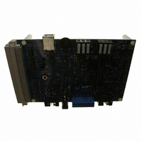
BOARD PROTOTYPE W/C8051F560
Manufacturer
Silicon Laboratories Inc
Type
MCUr
Datasheet
1.TOOLSTICK560DC.pdf
(302 pages)
Specifications of C8051F560-TB
Contents
Board
Processor To Be Evaluated
C8051F56x
Processor Series
C8051F56x
Interface Type
USB
Maximum Operating Temperature
+ 125 C
Minimum Operating Temperature
- 40 C
Operating Supply Voltage
1.8 V to 5.25 V
Lead Free Status / RoHS Status
Lead free / RoHS Compliant
For Use With/related Products
C8051F55x, C8051F56x, C8051F57x
For Use With
336-1691 - KIT DEVELOPMENT FOR C8051F560
Lead Free Status / Rohs Status
Lead free / RoHS Compliant
Other names
336-1694


C8051F55x/56x/57x
8.1. Comparator Multiplexer
C8051F55x/56x/57x devices include an analog input multiplexer for each of the comparators to connect
Port I/O pins to the comparator inputs. The Comparator0 inputs are selected in the CPT0MX register (SFR
Definition 8.5). The CMX0P3 – CMX0P0 bits select the Comparator0 positive input; the CMX0N3 – CMX0N0
bits select the Comparator0 negative input. Similarly, the Comparator1 inputs are selected in the CPT1MX
register using the CMX1P3-CMX1P0 bits and CMX1N3-CMX1N0 bits. The same pins are available to both
multiplexers at the same time and can be used by both comparators simultaneously.
Important Note About Comparator Inputs: The Port pins selected as comparator inputs should be con-
figured as analog inputs in their associated Port configuration register, and configured to be skipped by the
Crossbar (for details on Port configuration, see Section “19.6. Special Function Registers for Accessing
and Configuring Port I/O” on page 181).
76
P0.1
P0.3
P0.5
P0.7
P1.1
P1.3
P1.5
P1.7
P2.1
P2.3
P2.5
P2.7
CMXnN3
CMXnN2
CMXnN1
CMXnN0
CMXnP3
CMXnP2
CMXnP1
CMXnP0
Figure 8.3. Comparator Input Multiplexer Block Diagram
P0.0
P0.2
P0.4
P0.6
P1.0
P1.2
P1.4
P1.6
P2.0
P2.2
P2.4
P2.6
Rev. 1.1
CPn +
CPn -
+
-
VDD
GND
Related parts for C8051F560-TB
Image
Part Number
Description
Manufacturer
Datasheet
Request
R

Part Number:
Description:
SMD/C°/SINGLE-ENDED OUTPUT SILICON OSCILLATOR
Manufacturer:
Silicon Laboratories Inc
Part Number:
Description:
Manufacturer:
Silicon Laboratories Inc
Datasheet:
Part Number:
Description:
N/A N/A/SI4010 AES KEYFOB DEMO WITH LCD RX
Manufacturer:
Silicon Laboratories Inc
Datasheet:
Part Number:
Description:
N/A N/A/SI4010 SIMPLIFIED KEY FOB DEMO WITH LED RX
Manufacturer:
Silicon Laboratories Inc
Datasheet:
Part Number:
Description:
N/A/-40 TO 85 OC/EZLINK MODULE; F930/4432 HIGH BAND (REV E/B1)
Manufacturer:
Silicon Laboratories Inc
Part Number:
Description:
EZLink Module; F930/4432 Low Band (rev e/B1)
Manufacturer:
Silicon Laboratories Inc
Part Number:
Description:
I°/4460 10 DBM RADIO TEST CARD 434 MHZ
Manufacturer:
Silicon Laboratories Inc
Part Number:
Description:
I°/4461 14 DBM RADIO TEST CARD 868 MHZ
Manufacturer:
Silicon Laboratories Inc
Part Number:
Description:
I°/4463 20 DBM RFSWITCH RADIO TEST CARD 460 MHZ
Manufacturer:
Silicon Laboratories Inc
Part Number:
Description:
I°/4463 20 DBM RADIO TEST CARD 868 MHZ
Manufacturer:
Silicon Laboratories Inc
Part Number:
Description:
I°/4463 27 DBM RADIO TEST CARD 868 MHZ
Manufacturer:
Silicon Laboratories Inc
Part Number:
Description:
I°/4463 SKYWORKS 30 DBM RADIO TEST CARD 915 MHZ
Manufacturer:
Silicon Laboratories Inc
Part Number:
Description:
N/A N/A/-40 TO 85 OC/4463 RFMD 30 DBM RADIO TEST CARD 915 MHZ
Manufacturer:
Silicon Laboratories Inc
Part Number:
Description:
I°/4463 20 DBM RADIO TEST CARD 169 MHZ
Manufacturer:
Silicon Laboratories Inc