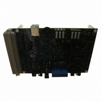
C8051F560-TB Silicon Laboratories Inc, C8051F560-TB Datasheet - Page 53

C8051F560-TB
Manufacturer Part Number
C8051F560-TB
Description
BOARD PROTOTYPE W/C8051F560
Manufacturer
Silicon Laboratories Inc
Type
MCUr
Datasheet
1.TOOLSTICK560DC.pdf
(302 pages)
Specifications of C8051F560-TB
Contents
Board
Processor To Be Evaluated
C8051F56x
Processor Series
C8051F56x
Interface Type
USB
Maximum Operating Temperature
+ 125 C
Minimum Operating Temperature
- 40 C
Operating Supply Voltage
1.8 V to 5.25 V
Lead Free Status / RoHS Status
Lead free / RoHS Compliant
For Use With/related Products
C8051F55x, C8051F56x, C8051F57x
For Use With
336-1691 - KIT DEVELOPMENT FOR C8051F560
Lead Free Status / Rohs Status
Lead free / RoHS Compliant
Other names
336-1694
- Current page: 53 of 302
- Download datasheet (3Mb)
6.3. Selectable Gain
ADC0 on the C8051F55x/56x/57x family of devices implements a selectable gain adjustment option. By
writing a value to the gain adjust address range, the user can select gain values between 0 and 1.016.
For example, three analog sources to be measured have full-scale outputs of 5.0 V, 4.0 V, and 3.0 V,
respectively. Each ADC measurement would ideally use the full dynamic range of the ADC with an internal
voltage reference of 1.5 V or 2.2 V (set to 2.2 V for this example). When selecting the first source (5.0 V
full-scale), a gain value of 0.44 (5 V full scale x 0.44 = 2.2 V full scale) provides a full-scale signal of 2.2 V
when the input signal is 5.0 V. Likewise, a gain value of 0.55 (4 V full scale x 0.55 = 2.2 V full scale) for the
second source and 0.73 (3 V full scale x 0.73 = 2.2 V full scale) for the third source provide full-scale ADC0
measurements when the input signal is full-scale.
Additionally, some sensors or other input sources have small part-to-part variations that must be
accounted for to achieve accurate results. In this case, the programmable gain value could be used as a
calibration value to eliminate these part-to-part variations.
6.3.1. Calculating the Gain Value
The ADC0 selectable gain feature is controlled by 13 bits in three registers. ADC0GNH contains the 8
upper bits of the gain value and ADC0GNL contains the 4 lower bits of the gain value. The final GAINADD
bit (ADC0GNA.0) controls an optional extra 1/64 (0.016) of gain that can be added in addition to the
ADC0GNH and ADC0GNL gain. The ADC0GNA.0 bit is set to 1 after a power-on reset.
The equivalent gain for the ADC0GNH, ADC0GNL and ADC0GNA registers is as follows:
Where:
GAIN is the 12-bit word of ADC0GNH[7:0] and ADC0GNL[7:4]
GAINADD is the value of the GAINADD bit (ADC0GNA.0)
gain is the equivalent gain value from 0 to 1.016
Equation 6.2. Equivalent Gain from the ADC0GNH and ADC0GNL Registers
P x . x
Figure 6.5. ADC0 Equivalent Input Circuit
gain
R C
M U X S e le c t
In p u t
=
= R
GAIN
-------------- -
4096
M U X
* C
+
Rev. 1.1
R
GAINADD
S A M P L E
M U X
C8051F55x/56x/57x
----- -
64
1
C
S A M P L E
53
Related parts for C8051F560-TB
Image
Part Number
Description
Manufacturer
Datasheet
Request
R
Part Number:
Description:
SMD/C°/SINGLE-ENDED OUTPUT SILICON OSCILLATOR
Manufacturer:
Silicon Laboratories Inc
Part Number:
Description:
Manufacturer:
Silicon Laboratories Inc
Datasheet:
Part Number:
Description:
N/A N/A/SI4010 AES KEYFOB DEMO WITH LCD RX
Manufacturer:
Silicon Laboratories Inc
Datasheet:
Part Number:
Description:
N/A N/A/SI4010 SIMPLIFIED KEY FOB DEMO WITH LED RX
Manufacturer:
Silicon Laboratories Inc
Datasheet:
Part Number:
Description:
N/A/-40 TO 85 OC/EZLINK MODULE; F930/4432 HIGH BAND (REV E/B1)
Manufacturer:
Silicon Laboratories Inc
Part Number:
Description:
EZLink Module; F930/4432 Low Band (rev e/B1)
Manufacturer:
Silicon Laboratories Inc
Part Number:
Description:
I°/4460 10 DBM RADIO TEST CARD 434 MHZ
Manufacturer:
Silicon Laboratories Inc
Part Number:
Description:
I°/4461 14 DBM RADIO TEST CARD 868 MHZ
Manufacturer:
Silicon Laboratories Inc
Part Number:
Description:
I°/4463 20 DBM RFSWITCH RADIO TEST CARD 460 MHZ
Manufacturer:
Silicon Laboratories Inc
Part Number:
Description:
I°/4463 20 DBM RADIO TEST CARD 868 MHZ
Manufacturer:
Silicon Laboratories Inc
Part Number:
Description:
I°/4463 27 DBM RADIO TEST CARD 868 MHZ
Manufacturer:
Silicon Laboratories Inc
Part Number:
Description:
I°/4463 SKYWORKS 30 DBM RADIO TEST CARD 915 MHZ
Manufacturer:
Silicon Laboratories Inc
Part Number:
Description:
N/A N/A/-40 TO 85 OC/4463 RFMD 30 DBM RADIO TEST CARD 915 MHZ
Manufacturer:
Silicon Laboratories Inc
Part Number:
Description:
I°/4463 20 DBM RADIO TEST CARD 169 MHZ
Manufacturer:
Silicon Laboratories Inc


