C8051F560-TB Silicon Laboratories Inc, C8051F560-TB Datasheet - Page 44
C8051F560-TB
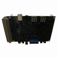
Manufacturer Part Number
C8051F560-TB
Description
BOARD PROTOTYPE W/C8051F560
Manufacturer
Silicon Laboratories Inc
Type
MCUr
Datasheet
1.TOOLSTICK560DC.pdf
(302 pages)
Specifications of C8051F560-TB
Contents
Board
Processor To Be Evaluated
C8051F56x
Processor Series
C8051F56x
Interface Type
USB
Maximum Operating Temperature
+ 125 C
Minimum Operating Temperature
- 40 C
Operating Supply Voltage
1.8 V to 5.25 V
Lead Free Status / RoHS Status
Lead free / RoHS Compliant
For Use With/related Products
C8051F55x, C8051F56x, C8051F57x
For Use With
336-1691 - KIT DEVELOPMENT FOR C8051F560
Lead Free Status / Rohs Status
Lead free / RoHS Compliant
Other names
336-1694


C8051F55x/56x/57x
Table 5.9. ADC0 Electrical Characteristics
VDDA
44
DC Accuracy
Resolution
Integral Nonlinearity
Differential Nonlinearity
Offset Error
Full Scale Error
Offset Temperature Coefficient
Dynamic performance (10 kHz sine-wave single-ended input, 1 dB below Full Scale, 200 ksps)
Signal-to-Noise Plus Distortion
Total Harmonic Distortion
Spurious-Free Dynamic Range
Conversion Rate
SAR Conversion Clock
Conversion Time in SAR Clocks
Track/Hold Acquisition Time
Throughput Rate
Analog Inputs
ADC Input Voltage Range
Absolute Pin Voltage with respect
to GND
Sampling Capacitance
Input Multiplexer Impedance
Power Specifications
Power Supply Current
(VDDA supplied to ADC0)
Burst Mode (Idle)
Power-On Time
Power Supply Rejection
Notes:
1. Represents one standard deviation from the mean. Offset and full-scale error can be removed through
2. An additional 2 FCLK cycles are required to start and complete a conversion
3. Additional tracking time may be required depending on the output impedance connected to the ADC input.
4. An increase in tracking time will decrease the ADC throughput.
5. See Section “
= 1.8 to 2.75 V, –40 to +125 °C, VREF = 1.5 V (REFSL=0) unless otherwise specified.
calibration.
See Section “
Parameter
1
4
6.2.1. Settling Time Requirements
6.3. Selectable Gain
5
3
2
Guaranteed Monotonic
Up to the 5th harmonic;
VDDA > 2.0 V
VDDA < 2.0 V
VDDA > 2.0 V
gain = 1.0 (default)
gain = n
Operating Mode, 200 ksps
” on page
Conditions
53
Rev. 1.1
for more information about the setting the gain.
” on page
52
.
Min
–10
–20
1.5
3.5
63
13
—
—
—
—
—
—
—
—
—
—
—
—
0
0
0
5
1100
1100
±0.5
±0.5
Typ
–60
-82
3.0
5.7
7.7
65
80
31
—
—
—
—
—
—
—
—
3
12
VREF / n
VREF
1500
1500
Max
200
V
3.6
±3
±1
10
20
—
—
—
—
—
—
—
—
—
—
—
IO
ppm/°C
clocks
Units
mV/V
MHz
ksps
LSB
LSB
LSB
LSB
bits
k
µA
µA
dB
dB
dB
pF
µs
µs
V
V
Related parts for C8051F560-TB
Image
Part Number
Description
Manufacturer
Datasheet
Request
R

Part Number:
Description:
SMD/C°/SINGLE-ENDED OUTPUT SILICON OSCILLATOR
Manufacturer:
Silicon Laboratories Inc
Part Number:
Description:
Manufacturer:
Silicon Laboratories Inc
Datasheet:
Part Number:
Description:
N/A N/A/SI4010 AES KEYFOB DEMO WITH LCD RX
Manufacturer:
Silicon Laboratories Inc
Datasheet:
Part Number:
Description:
N/A N/A/SI4010 SIMPLIFIED KEY FOB DEMO WITH LED RX
Manufacturer:
Silicon Laboratories Inc
Datasheet:
Part Number:
Description:
N/A/-40 TO 85 OC/EZLINK MODULE; F930/4432 HIGH BAND (REV E/B1)
Manufacturer:
Silicon Laboratories Inc
Part Number:
Description:
EZLink Module; F930/4432 Low Band (rev e/B1)
Manufacturer:
Silicon Laboratories Inc
Part Number:
Description:
I°/4460 10 DBM RADIO TEST CARD 434 MHZ
Manufacturer:
Silicon Laboratories Inc
Part Number:
Description:
I°/4461 14 DBM RADIO TEST CARD 868 MHZ
Manufacturer:
Silicon Laboratories Inc
Part Number:
Description:
I°/4463 20 DBM RFSWITCH RADIO TEST CARD 460 MHZ
Manufacturer:
Silicon Laboratories Inc
Part Number:
Description:
I°/4463 20 DBM RADIO TEST CARD 868 MHZ
Manufacturer:
Silicon Laboratories Inc
Part Number:
Description:
I°/4463 27 DBM RADIO TEST CARD 868 MHZ
Manufacturer:
Silicon Laboratories Inc
Part Number:
Description:
I°/4463 SKYWORKS 30 DBM RADIO TEST CARD 915 MHZ
Manufacturer:
Silicon Laboratories Inc
Part Number:
Description:
N/A N/A/-40 TO 85 OC/4463 RFMD 30 DBM RADIO TEST CARD 915 MHZ
Manufacturer:
Silicon Laboratories Inc
Part Number:
Description:
I°/4463 20 DBM RADIO TEST CARD 169 MHZ
Manufacturer:
Silicon Laboratories Inc