C8051F560-TB Silicon Laboratories Inc, C8051F560-TB Datasheet - Page 93
C8051F560-TB
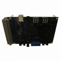
Manufacturer Part Number
C8051F560-TB
Description
BOARD PROTOTYPE W/C8051F560
Manufacturer
Silicon Laboratories Inc
Type
MCUr
Datasheet
1.TOOLSTICK560DC.pdf
(302 pages)
Specifications of C8051F560-TB
Contents
Board
Processor To Be Evaluated
C8051F56x
Processor Series
C8051F56x
Interface Type
USB
Maximum Operating Temperature
+ 125 C
Minimum Operating Temperature
- 40 C
Operating Supply Voltage
1.8 V to 5.25 V
Lead Free Status / RoHS Status
Lead free / RoHS Compliant
For Use With/related Products
C8051F55x, C8051F56x, C8051F57x
For Use With
336-1691 - KIT DEVELOPMENT FOR C8051F560
Lead Free Status / Rohs Status
Lead free / RoHS Compliant
Other names
336-1694


11.1.1. MOVX Instruction and Program Memory
The MOVX instruction in an 8051 device is typically used to access external data memory. On the
C8051F55x/56x/57x devices, the MOVX instruction is normally used to read and write on-chip XRAM, but
can be re-configured to write and erase on-chip Flash memory space. MOVC instructions are always used
to read Flash memory, while MOVX write instructions are used to erase and write Flash. This Flash access
feature provides a mechanism for the C8051F55x/56x/57x to update program code and use the program
memory space for non-volatile data storage. Refer to Section “14. Flash Memory” on page 124 for further
details.
11.2. Data Memory
The C8051F55x/56x/57x devices include 2304 bytes of RAM data memory. 256 bytes of this memory is
mapped into the internal RAM space of the 8051. The other 2048 bytes of this memory is on-chip “exter-
nal” memory. The data memory map is shown in Figure 11.1 for reference.
11.2.1. Internal RAM
There are 256 bytes of internal RAM mapped into the data memory space from 0x00 through 0xFF. The
lower 128 bytes of data memory are used for general purpose registers and scratch pad memory. Either
direct or indirect addressing may be used to access the lower 128 bytes of data memory. Locations 0x00
through 0x1F are addressable as four banks of general purpose registers, each bank consisting of eight
byte-wide registers. The next 16 bytes, locations 0x20 through 0x2F, may either be addressed as bytes or
as 128 bit locations accessible with the direct addressing mode.
The upper 128 bytes of data memory are accessible only by indirect addressing. This region occupies the
same address space as the Special Function Registers (SFR) but is physically separate from the SFR
space. The addressing mode used by an instruction when accessing locations above 0x7F determines
whether the CPU accesses the upper 128 bytes of data memory space or the SFRs. Instructions that use
direct addressing will access the SFR space. Instructions using indirect addressing above 0x7F access the
Flash Memory Space
(32 kB Flash Device)
C8051F550/1/2/3
C8051F560/1/2/3/8/9
C8051F570/1
Lock Byte Page
Reserved Area
Lock Byte
Figure 11.2. Flash Program Memory Map
0x7FFF
0x7C00
0x7BFF
0x7BFE
0x7A00
0x0000
Rev. 1.1
Flash Memory Space
(16 kB Flash Device)
C8051F554/5/6/7
C8051F564/5/6/7
C8051F572/3/4/5
Lock Byte Page
Lock Byte
C8051F55x/56x/57x
0x3FFF
0x3FFE
0x3E00
0x0000
93
Related parts for C8051F560-TB
Image
Part Number
Description
Manufacturer
Datasheet
Request
R

Part Number:
Description:
SMD/C°/SINGLE-ENDED OUTPUT SILICON OSCILLATOR
Manufacturer:
Silicon Laboratories Inc
Part Number:
Description:
Manufacturer:
Silicon Laboratories Inc
Datasheet:
Part Number:
Description:
N/A N/A/SI4010 AES KEYFOB DEMO WITH LCD RX
Manufacturer:
Silicon Laboratories Inc
Datasheet:
Part Number:
Description:
N/A N/A/SI4010 SIMPLIFIED KEY FOB DEMO WITH LED RX
Manufacturer:
Silicon Laboratories Inc
Datasheet:
Part Number:
Description:
N/A/-40 TO 85 OC/EZLINK MODULE; F930/4432 HIGH BAND (REV E/B1)
Manufacturer:
Silicon Laboratories Inc
Part Number:
Description:
EZLink Module; F930/4432 Low Band (rev e/B1)
Manufacturer:
Silicon Laboratories Inc
Part Number:
Description:
I°/4460 10 DBM RADIO TEST CARD 434 MHZ
Manufacturer:
Silicon Laboratories Inc
Part Number:
Description:
I°/4461 14 DBM RADIO TEST CARD 868 MHZ
Manufacturer:
Silicon Laboratories Inc
Part Number:
Description:
I°/4463 20 DBM RFSWITCH RADIO TEST CARD 460 MHZ
Manufacturer:
Silicon Laboratories Inc
Part Number:
Description:
I°/4463 20 DBM RADIO TEST CARD 868 MHZ
Manufacturer:
Silicon Laboratories Inc
Part Number:
Description:
I°/4463 27 DBM RADIO TEST CARD 868 MHZ
Manufacturer:
Silicon Laboratories Inc
Part Number:
Description:
I°/4463 SKYWORKS 30 DBM RADIO TEST CARD 915 MHZ
Manufacturer:
Silicon Laboratories Inc
Part Number:
Description:
N/A N/A/-40 TO 85 OC/4463 RFMD 30 DBM RADIO TEST CARD 915 MHZ
Manufacturer:
Silicon Laboratories Inc
Part Number:
Description:
I°/4463 20 DBM RADIO TEST CARD 169 MHZ
Manufacturer:
Silicon Laboratories Inc