C8051F560-TB Silicon Laboratories Inc, C8051F560-TB Datasheet - Page 170
C8051F560-TB
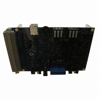
Manufacturer Part Number
C8051F560-TB
Description
BOARD PROTOTYPE W/C8051F560
Manufacturer
Silicon Laboratories Inc
Type
MCUr
Datasheet
1.TOOLSTICK560DC.pdf
(302 pages)
Specifications of C8051F560-TB
Contents
Board
Processor To Be Evaluated
C8051F56x
Processor Series
C8051F56x
Interface Type
USB
Maximum Operating Temperature
+ 125 C
Minimum Operating Temperature
- 40 C
Operating Supply Voltage
1.8 V to 5.25 V
Lead Free Status / RoHS Status
Lead free / RoHS Compliant
For Use With/related Products
C8051F55x, C8051F56x, C8051F57x
For Use With
336-1691 - KIT DEVELOPMENT FOR C8051F560
Lead Free Status / Rohs Status
Lead free / RoHS Compliant
Other names
336-1694


C8051F55x/56x/57x
19.2.3. Assigning Port I/O Pins to External Digital Event Capture Functions
External digital event capture functions can be used to trigger an interrupt or wake the device from a low
power mode when a transition occurs on a digital I/O pin. The digital event capture functions do not require
dedicated pins and will function on both GPIO pins (PnSKIP = 1) and pins in use by the Crossbar (PnSKIP
= 0). External digital event capture functions cannot be used on pins configured for analog I/O. Table 19.3
shows all available external digital event capture functions.
19.3. Priority Crossbar Decoder
The Priority Crossbar Decoder (Figure 19.3) assigns a priority to each I/O function, starting at the top with
UART0. When a digital resource is selected, the least-significant unassigned Port pin is assigned to that
resource excluding UART0, which is always assigned to pins P0.4 and P0.5, and excluding CAN0 which is
always assigned to pins P0.6 and P0.7. If a Port pin is assigned, the Crossbar skips that pin when assign-
ing the next selected resource. Additionally, the Crossbar will skip Port pins whose associated bits in the
PnSKIP registers are set. The PnSKIP registers allow software to skip Port pins that are to be used for
analog input, dedicated functions, or GPIO.
Because of the nature of Priority Crossbar Decoder, not all peripherals can be located on all port pins.
Figure 19.3 maps peripherals to the potential port pins on which the peripheral I/O can appear.
Important Note on Crossbar Configuration: If a Port pin is claimed by a peripheral without use of the
Crossbar, its corresponding PnSKIP bit should be set. This applies to P0.0 if VREF is used, P0.1 if the
ADC is configured to use the external conversion start signal (CNVSTR), P0.3 and/or P0.2 if the external
oscillator circuit is enabled, and any selected ADC or Comparator inputs. The Crossbar skips selected pins
as if they were already assigned, and moves to the next unassigned pin.
170
Digital Function
Any pin used for GPIO
*Note: P3.1–P3.7 are available on the 40-pin packages. P2.2-P3.0 are available 40-pin and 32-pin packages.
Digital Function
External Interrupt 0
External Interrupt 1
Port Match
*Note: P3.1–P3.7 are available on the 40-pin packages. P2.2-P3.0 are available 40-pin and 32-pin packages
Table 19.3. Port I/O Assignment for External Digital Event Capture Functions
Table 19.2. Port I/O Assignment for Digital Functions
Potentially Assignable Port Pins
Potentially Assignable Port Pins
Rev. 1.1
P0.0–P4.0*
P0.0–P3.7*
P1.0–P1.7
P1.0–P1.7
P0MASK, P0MAT
P1MASK, P1MAT
P2MASK, P2MAT
P3MASK, P3MAT
P0SKIP, P1SKIP,
SFR(s) used for
P2SKIP, P3SKIP
SFR(s) used for
Assignment
Assignment
IT01CF
IT01CF
Related parts for C8051F560-TB
Image
Part Number
Description
Manufacturer
Datasheet
Request
R

Part Number:
Description:
SMD/C°/SINGLE-ENDED OUTPUT SILICON OSCILLATOR
Manufacturer:
Silicon Laboratories Inc
Part Number:
Description:
Manufacturer:
Silicon Laboratories Inc
Datasheet:
Part Number:
Description:
N/A N/A/SI4010 AES KEYFOB DEMO WITH LCD RX
Manufacturer:
Silicon Laboratories Inc
Datasheet:
Part Number:
Description:
N/A N/A/SI4010 SIMPLIFIED KEY FOB DEMO WITH LED RX
Manufacturer:
Silicon Laboratories Inc
Datasheet:
Part Number:
Description:
N/A/-40 TO 85 OC/EZLINK MODULE; F930/4432 HIGH BAND (REV E/B1)
Manufacturer:
Silicon Laboratories Inc
Part Number:
Description:
EZLink Module; F930/4432 Low Band (rev e/B1)
Manufacturer:
Silicon Laboratories Inc
Part Number:
Description:
I°/4460 10 DBM RADIO TEST CARD 434 MHZ
Manufacturer:
Silicon Laboratories Inc
Part Number:
Description:
I°/4461 14 DBM RADIO TEST CARD 868 MHZ
Manufacturer:
Silicon Laboratories Inc
Part Number:
Description:
I°/4463 20 DBM RFSWITCH RADIO TEST CARD 460 MHZ
Manufacturer:
Silicon Laboratories Inc
Part Number:
Description:
I°/4463 20 DBM RADIO TEST CARD 868 MHZ
Manufacturer:
Silicon Laboratories Inc
Part Number:
Description:
I°/4463 27 DBM RADIO TEST CARD 868 MHZ
Manufacturer:
Silicon Laboratories Inc
Part Number:
Description:
I°/4463 SKYWORKS 30 DBM RADIO TEST CARD 915 MHZ
Manufacturer:
Silicon Laboratories Inc
Part Number:
Description:
N/A N/A/-40 TO 85 OC/4463 RFMD 30 DBM RADIO TEST CARD 915 MHZ
Manufacturer:
Silicon Laboratories Inc
Part Number:
Description:
I°/4463 20 DBM RADIO TEST CARD 169 MHZ
Manufacturer:
Silicon Laboratories Inc