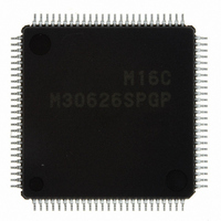
M30626SPGP#U3C Renesas Electronics America, M30626SPGP#U3C Datasheet - Page 391

M30626SPGP#U3C
Manufacturer Part Number
M30626SPGP#U3C
Description
IC M16C/62P MCU ROMLESS 100LQFP
Manufacturer
Renesas Electronics America
Series
M16C™ M16C/60r
Datasheet
1.M30620SPGPU3C.pdf
(423 pages)
Specifications of M30626SPGP#U3C
Core Processor
M16C/60
Core Size
16-Bit
Speed
24MHz
Connectivity
I²C, IEBus, UART/USART
Peripherals
DMA, WDT
Number Of I /o
50
Program Memory Type
ROMless
Ram Size
31K x 8
Voltage - Supply (vcc/vdd)
2.7 V ~ 5.5 V
Data Converters
A/D 26x10b; D/A 2x8b
Oscillator Type
Internal
Operating Temperature
-40°C ~ 85°C
Package / Case
100-LQFP
For Use With
867-1000 - KIT QUICK START RENESAS 62PR0K33062PS001BE - R0K33062P STARTER KITR0K33062PS000BE - KIT EVAL STARTER FOR M16C/62PM3062PT3-CPE-3 - EMULATOR COMPACT M16C/62P/30P
Lead Free Status / RoHS Status
Lead free / RoHS Compliant
Eeprom Size
-
Program Memory Size
-
Available stocks
Company
Part Number
Manufacturer
Quantity
Price
- Current page: 391 of 423
- Download datasheet (5Mb)
M16C/62P Group (M16C/62P, M16C/62PT)
Rev.2.41
REJ09B0185-0241
24.10.2 UART
24.10.3 SI/O3, SI/O4
24.10.2.1 Special Mode 1(I
24.10.2.2 Special Mode 2
24.10.2.3 Special Mode 4 (SIM Mode)
When generating start, stop and restart conditions, set the STSPSEL bit in the UiSMR4 register to “0” and wait
for more than half cycle of the transfer clock before setting each condition generate bit (STAREQ, RSTAREQ
and STPREQ) from “0” to “1”.
If a low-level signal is applied to the NMI pin when the IVPCR1 bit in the TB2SC register = 1 (three-phase
output forcible cutoff by input on NMI pin enabled), the RTS2 and CLK2 pins go to a high-impedance state.
A transmit interrupt request is generated by setting the U2C1 register U2IRS bit to “1” (transmission complete)
and U2ERE bit to “1” (error signal output) after reset is deasserted. Therefore, when using SIM mode, be sure
to clear the IR bit to “0” (no interrupt request) after setting these bits.
The SOUTi default value which is set to the SOUTi pin by the SMi7 bit approximately 10ns may be output
when changing the SMi3 bit from “0” (I/O port) to “1” (SOUTi output and CLK function) while the SMi2 bit in
the SiC (i=3 and 4) to “0” (SOUTi output) and the SMi6 bit is set to “1” (internal clock). And then the SOUTi
pin is held high-impedance.
If the level which is output from the SOUTi pin is a problem when changing the SMi3 bit from “0” to “1”, set
the default value of the SOUTi pin by the SMi7 bit.
Jan 10, 2006
Page 374 of 390
2
C Mode)
24. Precautions
Related parts for M30626SPGP#U3C
Image
Part Number
Description
Manufacturer
Datasheet
Request
R

Part Number:
Description:
KIT STARTER FOR M16C/29
Manufacturer:
Renesas Electronics America
Datasheet:

Part Number:
Description:
KIT STARTER FOR R8C/2D
Manufacturer:
Renesas Electronics America
Datasheet:

Part Number:
Description:
R0K33062P STARTER KIT
Manufacturer:
Renesas Electronics America
Datasheet:

Part Number:
Description:
KIT STARTER FOR R8C/23 E8A
Manufacturer:
Renesas Electronics America
Datasheet:

Part Number:
Description:
KIT STARTER FOR R8C/25
Manufacturer:
Renesas Electronics America
Datasheet:

Part Number:
Description:
KIT STARTER H8S2456 SHARPE DSPLY
Manufacturer:
Renesas Electronics America
Datasheet:

Part Number:
Description:
KIT STARTER FOR R8C38C
Manufacturer:
Renesas Electronics America
Datasheet:

Part Number:
Description:
KIT STARTER FOR R8C35C
Manufacturer:
Renesas Electronics America
Datasheet:

Part Number:
Description:
KIT STARTER FOR R8CL3AC+LCD APPS
Manufacturer:
Renesas Electronics America
Datasheet:

Part Number:
Description:
KIT STARTER FOR RX610
Manufacturer:
Renesas Electronics America
Datasheet:

Part Number:
Description:
KIT STARTER FOR R32C/118
Manufacturer:
Renesas Electronics America
Datasheet:

Part Number:
Description:
KIT DEV RSK-R8C/26-29
Manufacturer:
Renesas Electronics America
Datasheet:

Part Number:
Description:
KIT STARTER FOR SH7124
Manufacturer:
Renesas Electronics America
Datasheet:

Part Number:
Description:
KIT STARTER FOR H8SX/1622
Manufacturer:
Renesas Electronics America
Datasheet:

Part Number:
Description:
KIT DEV FOR SH7203
Manufacturer:
Renesas Electronics America
Datasheet:


