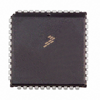
MC68HC705C8ACFNE Freescale Semiconductor, MC68HC705C8ACFNE Datasheet - Page 101

MC68HC705C8ACFNE
Manufacturer Part Number
MC68HC705C8ACFNE
Description
IC MCU 8K 2.1MHZ OTP 44-PLCC
Manufacturer
Freescale Semiconductor
Series
HC05r
Datasheet
1.MC68HC705C8AB.pdf
(222 pages)
Specifications of MC68HC705C8ACFNE
Core Processor
HC05
Core Size
8-Bit
Speed
2.1MHz
Connectivity
SCI, SPI
Peripherals
POR, WDT
Number Of I /o
24
Program Memory Size
8KB (8K x 8)
Program Memory Type
OTP
Ram Size
304 x 8
Voltage - Supply (vcc/vdd)
3 V ~ 5.5 V
Oscillator Type
Internal
Operating Temperature
-40°C ~ 85°C
Package / Case
44-PLCC
A/d Inputs
4-Channel, 8-Bit
Eeprom Memory
0 Bytes
Input Output
24
Interface
SCI/SPI
Memory Type
OTP
Number Of Bits
8
Package Type
44-pin PLCC
Programmable Memory
8K Bytes
Timers
3-16-bit
Voltage, Range
3-5.5 V
Processor Series
HC705C
Core
HC05
Data Bus Width
8 bit
Data Ram Size
304 B
Interface Type
SCI, SPI
Maximum Clock Frequency
2.1 MHz
Number Of Programmable I/os
24
Number Of Timers
1
Maximum Operating Temperature
+ 85 C
Mounting Style
SMD/SMT
Minimum Operating Temperature
- 40 C
On-chip Adc
8 bit
Lead Free Status / RoHS Status
Lead free / RoHS Compliant
Eeprom Size
-
Data Converters
-
Lead Free Status / Rohs Status
RoHS Compliant part
Available stocks
Company
Part Number
Manufacturer
Quantity
Price
Company:
Part Number:
MC68HC705C8ACFNE
Manufacturer:
Freescale Semiconductor
Quantity:
10 000
Part Number:
MC68HC705C8ACFNE
Manufacturer:
FREESCALE
Quantity:
20 000
8.4.6 Output Compare Registers
MC68HC705C8A — Rev. 3
MOTOROLA
Register Name and Address: Output Compare Register High — $0016
Register Name and Address: Output Compare Register Low — $0017
When the value of the 16-bit counter matches the value in the read/write
output compare registers (OCRH and OCRL) shown in
planned TCMP pin action takes place. Writing to OCRH before writing to
OCRL inhibits timer compares until OCRL is written. Reading or writing
to OCRL after reading the timer status register clears the output
compare flag (OCF).
To prevent OCF from being set between the time it is read and the time
the output compare registers are updated, use this procedure:
Reset:
Reset:
Read:
Read:
Write:
Write:
1. Disable interrupts by setting the I bit in the condition code register.
2. Write to OCRH. Compares are now inhibited until OCRL is written.
3. Clear bit OCF by reading the timer status register (TSR).
4. Enable the output compare function by writing to OCRL.
5. Enable interrupts by clearing the I bit in the condition code register.
Freescale Semiconductor, Inc.
Figure 8-12. Output Compare Registers (OCRH and OCRL)
For More Information On This Product,
Bit 15
Bit 7
Bit 7
Go to: www.freescale.com
Capture/Compare Timer
Bit 14
Bit 6
6
Bit 13
Bit 5
5
Unaffected by reset
Unaffected by reset
Bit 12
Bit 4
4
Bit 11
Bit 3
3
Bit 10
Bit 2
2
Capture/Compare Timer
Figure
Timer I/O Registers
Bit 9
Bit 1
1
Technical Data
8-12, the
Bit 0
Bit 8
Bit 0


