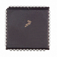
MC68HC705C8ACFNE Freescale Semiconductor, MC68HC705C8ACFNE Datasheet - Page 36

MC68HC705C8ACFNE
Manufacturer Part Number
MC68HC705C8ACFNE
Description
IC MCU 8K 2.1MHZ OTP 44-PLCC
Manufacturer
Freescale Semiconductor
Series
HC05r
Datasheet
1.MC68HC705C8AB.pdf
(222 pages)
Specifications of MC68HC705C8ACFNE
Core Processor
HC05
Core Size
8-Bit
Speed
2.1MHz
Connectivity
SCI, SPI
Peripherals
POR, WDT
Number Of I /o
24
Program Memory Size
8KB (8K x 8)
Program Memory Type
OTP
Ram Size
304 x 8
Voltage - Supply (vcc/vdd)
3 V ~ 5.5 V
Oscillator Type
Internal
Operating Temperature
-40°C ~ 85°C
Package / Case
44-PLCC
A/d Inputs
4-Channel, 8-Bit
Eeprom Memory
0 Bytes
Input Output
24
Interface
SCI/SPI
Memory Type
OTP
Number Of Bits
8
Package Type
44-pin PLCC
Programmable Memory
8K Bytes
Timers
3-16-bit
Voltage, Range
3-5.5 V
Processor Series
HC705C
Core
HC05
Data Bus Width
8 bit
Data Ram Size
304 B
Interface Type
SCI, SPI
Maximum Clock Frequency
2.1 MHz
Number Of Programmable I/os
24
Number Of Timers
1
Maximum Operating Temperature
+ 85 C
Mounting Style
SMD/SMT
Minimum Operating Temperature
- 40 C
On-chip Adc
8 bit
Lead Free Status / RoHS Status
Lead free / RoHS Compliant
Eeprom Size
-
Data Converters
-
Lead Free Status / Rohs Status
RoHS Compliant part
Available stocks
Company
Part Number
Manufacturer
Quantity
Price
Company:
Part Number:
MC68HC705C8ACFNE
Manufacturer:
Freescale Semiconductor
Quantity:
10 000
Part Number:
MC68HC705C8ACFNE
Manufacturer:
FREESCALE
Quantity:
20 000
Memory
2.4 Input/Output (I/O)
2.5 RAM
Technical Data
36
NOTE:
subroutine call to save the CPU state. The stack pointer decrements
during pushes and increments during pulls.
Figure 2-1
shown in
registers. Additional I/O registers have these addresses:
The first 32 addresses of memory space, from $0000 to $001F, are the
I/O section. These are the addresses of the I/O control registers, status
registers, and data registers. See
One of four selectable memory configurations is selected by the state of
the RAM1 and RAM0 bits in the option register located at $1FDF. Reset
or power-on reset (POR) clears these bits, automatically selecting the
first memory configuration as shown in
Register.
Be careful when using nested subroutines or multiple interrupt levels.
The CPU can overwrite data in the stack RAM during a subroutine or
during the interrupt stacking operation.
•
•
•
Freescale Semiconductor, Inc.
For More Information On This Product,
$1FDF, option register
$1FF0, mask option register 1 (MOR1)
$1FF1, mask option register 2 (MOR2)
Figure
is a memory map of the MCU. Addresses $0000–$001F,
Go to: www.freescale.com
RAM0
0
1
0
1
2-2, contain most of the control, status, and data
Table 2-1. Memory Configurations
Memory
RAM1
0
0
1
1
Figure 2-2
RAM Bytes
176
208
272
304
Table
for more information.
2-1. See
MC68HC705C8A — Rev. 3
PROM Bytes
7744
7696
7648
7600
9.5.1 Option


