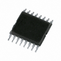
SC18IS602BIPW,112 NXP Semiconductors, SC18IS602BIPW,112 Datasheet - Page 11

SC18IS602BIPW,112
Manufacturer Part Number
SC18IS602BIPW,112
Description
IC BRIDGE SPI/I2C 16-TSSOP
Manufacturer
NXP Semiconductors
Specifications of SC18IS602BIPW,112
Controller Type
I²C Bus Controller
Interface
I²C
Voltage - Supply
2.4 V ~ 3.6 V
Current - Supply
11mA
Operating Temperature
-40°C ~ 85°C
Mounting Type
Surface Mount
Package / Case
16-TSSOP
Operating Temperature Classification
Military
Operating Temperature (max)
125C
Package Type
TSSOP
Rad Hardened
No
Maximum Operating Frequency
4.5 MHz
Maximum Operating Temperature
+ 125 C
Minimum Operating Temperature
- 55 C
Mounting Style
SMD/SMT
Supply Voltage (max)
3.6 V
Supply Voltage (min)
2.4 V
For Use With
568-4705 - DEMO BOARD I2C TO SPI SC18IS602
Lead Free Status / RoHS Status
Lead free / RoHS Compliant
Other names
568-4785-5
935286182112
SC18IS602BIPW
SC18IS602BIPW,112
SC18IS602BIPW
935286182112
SC18IS602BIPW
SC18IS602BIPW,112
SC18IS602BIPW
Available stocks
Company
Part Number
Manufacturer
Quantity
Price
Company:
Part Number:
SC18IS602BIPW,112
Manufacturer:
NXP
Quantity:
463
NXP Semiconductors
SC18IS602_602B_603_4
Product data sheet
7.1.11.2 Open-drain output configuration
A second pull-up, called the ‘weak’ pull-up, is turned on when the port latch for the pin
contains a logic 1 and the pin itself is also at a logic 1 level. This pull-up provides the
primary source current for a quasi-bidirectional pin that is outputting a 1. If this pin is
pulled LOW by an external device, the weak pull-up turns off, and only the very weak
pull-up remains on. In order to pull the pin LOW under these conditions, the external
device has to sink enough current to overpower the weak pull-up and pull the pin below its
input threshold voltage.
The third pull-up is referred to as the ‘strong’ pull-up. This pull-up is used to speed up
LOW-to-HIGH transitions on a quasi-bidirectional pin when the port latch changes from a
logic 0 to a logic 1. When this occurs, the strong pull-up turns on for two CPU clocks
quickly pulling the pin HIGH.
The quasi-bidirectional pin configuration is shown in
Although the SC18IS602/602B/603 is a 3 V device, most of the pins are 5 V tolerant. If 5 V
is applied to a pin configured in quasi-bidirectional mode, there will be a current flowing
from the pin to V
configured in quasi-bidirectional mode is discouraged.
A quasi-bidirectional pin has a Schmitt-triggered input that also has a glitch suppression
circuit.
The open-drain output configuration turns off all pull-ups and only drives the pull-down
transistor of the pin when the port latch contains a logic 0. To be used as a logic output, a
pin configured in this manner must have an external pull-up, typically a resistor tied to
V
The open-drain pin configuration is shown in
An open-drain pin has a Schmitt-triggered input that also has a glitch suppression circuit.
Fig 16. Quasi-bidirectional output configuration
DD
. The pull-down for this mode is the same as for the quasi-bidirectional mode.
pin latch data
DD
causing extra power consumption. Therefore, applying 5 V to pins
Rev. 04 — 11 March 2008
2 SYSTEM
CYCLES
CLOCK
Figure
P
input data
SC18IS602/602B/603
V
SS
strong
17.
Figure
P
very
weak
16.
P
glitch rejection
I
2
C-bus to SPI bridge
weak
© NXP B.V. 2008. All rights reserved.
V
DD
002aac548
GPIO pin
11 of 25


