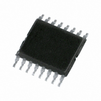
SC18IS602BIPW,112 NXP Semiconductors, SC18IS602BIPW,112 Datasheet - Page 9

SC18IS602BIPW,112
Manufacturer Part Number
SC18IS602BIPW,112
Description
IC BRIDGE SPI/I2C 16-TSSOP
Manufacturer
NXP Semiconductors
Specifications of SC18IS602BIPW,112
Controller Type
I²C Bus Controller
Interface
I²C
Voltage - Supply
2.4 V ~ 3.6 V
Current - Supply
11mA
Operating Temperature
-40°C ~ 85°C
Mounting Type
Surface Mount
Package / Case
16-TSSOP
Operating Temperature Classification
Military
Operating Temperature (max)
125C
Package Type
TSSOP
Rad Hardened
No
Maximum Operating Frequency
4.5 MHz
Maximum Operating Temperature
+ 125 C
Minimum Operating Temperature
- 55 C
Mounting Style
SMD/SMT
Supply Voltage (max)
3.6 V
Supply Voltage (min)
2.4 V
For Use With
568-4705 - DEMO BOARD I2C TO SPI SC18IS602
Lead Free Status / RoHS Status
Lead free / RoHS Compliant
Other names
568-4785-5
935286182112
SC18IS602BIPW
SC18IS602BIPW,112
SC18IS602BIPW
935286182112
SC18IS602BIPW
SC18IS602BIPW,112
SC18IS602BIPW
Available stocks
Company
Part Number
Manufacturer
Quantity
Price
Company:
Part Number:
SC18IS602BIPW,112
Manufacturer:
NXP
Quantity:
463
NXP Semiconductors
SC18IS602_602B_603_4
Product data sheet
7.1.10 GPIO Enable - Function ID F6h
7.1.9 GPIO Read - Function ID F5h
The state of the pins defined as GPIO may be read into the SC18IS602/602B/603 data
buffer using the GPIO Read function.
Note that this function does not return the value of the GPIO. To receive the GPIO
contents, a one-byte Read Buffer command would be required. The value of the Read
Buffer command will return the following byte.
Table 7.
[1]
Data for pins not defined as GPIO are undefined.
A GPIO Read is always performed to update the GPIO data in the buffer. The buffer is
undefined after the GPIO data is read back from the buffer. Therefore, reading data from
the GPIO always requires a two-message sequence (GPIO Read, followed by Read
Buffer).
At reset, the Slave Select pins (SS0, SS1, SS2 and SS3) are configured to be used as
slave select outputs. If these pins are not required for the SPI functions, they can be used
as GPIO after they are enabled as GPIO. Any combination of pins may be configured to
function as GPIO or Slave Selects.
After the GPIO Enable function is sent, the ports defined as GPIO will be configured as
quasi-bidirectional.
The data byte following the F6h command byte will determine which pins can be used as
GPIO. A logic 1 will enable the pin as a GPIO, while a logic 0 will disable GPIO control.
Table 8.
[1]
Fig 14. GPIO Read
Fig 15. GPIO Enable
SS3 does not exist in the SC18IS603.
SS3 does not exist in the SC18IS603.
X
X
7
7
GPIO Read (F5h) bit allocation
GPIO Enable (F6h) bit allocation
X
X
6
6
S
S
SLAVE ADDRESS
SLAVE ADDRESS
Rev. 04 — 11 March 2008
X
X
5
5
W
W
X
X
4
4
A
A
SC18IS602/602B/603
F5h
F6h
SS3
SS3
3
3
[1]
[1]
A
A
DATA
DATA
SS2
SS2
2
2
002aac455
002aac456
I
2
A
A
C-bus to SPI bridge
P
P
SS1
SS1
© NXP B.V. 2008. All rights reserved.
1
1
SS0
SS0
0
0
9 of 25


