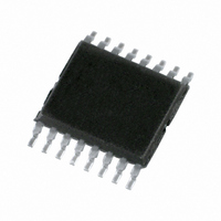
SC18IS602BIPW,112 NXP Semiconductors, SC18IS602BIPW,112 Datasheet - Page 7

SC18IS602BIPW,112
Manufacturer Part Number
SC18IS602BIPW,112
Description
IC BRIDGE SPI/I2C 16-TSSOP
Manufacturer
NXP Semiconductors
Specifications of SC18IS602BIPW,112
Controller Type
I²C Bus Controller
Interface
I²C
Voltage - Supply
2.4 V ~ 3.6 V
Current - Supply
11mA
Operating Temperature
-40°C ~ 85°C
Mounting Type
Surface Mount
Package / Case
16-TSSOP
Operating Temperature Classification
Military
Operating Temperature (max)
125C
Package Type
TSSOP
Rad Hardened
No
Maximum Operating Frequency
4.5 MHz
Maximum Operating Temperature
+ 125 C
Minimum Operating Temperature
- 55 C
Mounting Style
SMD/SMT
Supply Voltage (max)
3.6 V
Supply Voltage (min)
2.4 V
For Use With
568-4705 - DEMO BOARD I2C TO SPI SC18IS602
Lead Free Status / RoHS Status
Lead free / RoHS Compliant
Other names
568-4785-5
935286182112
SC18IS602BIPW
SC18IS602BIPW,112
SC18IS602BIPW
935286182112
SC18IS602BIPW
SC18IS602BIPW,112
SC18IS602BIPW
Available stocks
Company
Part Number
Manufacturer
Quantity
Price
Company:
Part Number:
SC18IS602BIPW,112
Manufacturer:
NXP
Quantity:
463
NXP Semiconductors
SC18IS602_602B_603_4
Product data sheet
7.1.5 Configure SPI Interface - Function ID F0h
The SPI hardware operating mode, data direction, and frequency can be changed by
sending a ‘Configure SPI Interface’ command to the I
After the SC18IS602/602B/603 address is transmitted on the bus, the Configure SPI
Interface Function ID (F0h) is sent followed by a byte which will define the SPI
communications.
The Clock Phase bit (CPHA) allows the user to set the edges for sampling and changing
data. The Clock Polarity bit (CPOL) allows the user to set the clock polarity.
Figure 21
Table 4.
Table 5.
Bit
Symbol
Reset
Bit
7:6
5
4
3:2
1:0
Fig 10. Configure SPI Interface
show the different settings of Clock Phase bit CPHA.
Symbol
-
ORDER
-
MODE1:MODE0 Mode selection
F1:F0
Configure SPI Interface (F0h) bit allocation
Configure SPI Interface (F0h) bit description
X
X
7
S
SLAVE ADDRESS
Rev. 04 — 11 March 2008
6
X
X
Description
reserved
When logic 0, the MSB of the data word is transmitted first.
If logic 1, the LSB of the data word is transmitted first.
reserved
SPI clock rate
SC18IS602/602B:
SC18IS603:
00 - SPICLK LOW when idle; data clocked in on leading edge
(CPOL = 0, CPHA = 0)
01 - SPICLK LOW when idle; data clocked in on trailing edge
(CPOL = 0, CPHA = 1)
10 - SPICLK HIGH when idle; data clocked in on trailing edge
(CPOL = 1, CPHA = 0)
11 - SPICLK HIGH when idle; data clocked in on leading edge
(CPOL = 1, CPHA = 1)
00 - 1843 kHz
01 - 461 kHz
10 - 115 kHz
11 - 58 kHz
00 -
01 -
10 -
11 -
ORDER
fosc
fosc
fosc
fosc
5
0
4
16
64
128
W
A
X
X
4
SC18IS602/602B/603
F0h
MODE1
2
A
3
0
C-bus.
DATA
MODE0
2
0
002aac450
I
2
A
C-bus to SPI bridge
P
© NXP B.V. 2008. All rights reserved.
F1
1
0
Figure 20
F0
0
0
7 of 25
and


