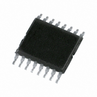
SC18IS602BIPW,112 NXP Semiconductors, SC18IS602BIPW,112 Datasheet - Page 13

SC18IS602BIPW,112
Manufacturer Part Number
SC18IS602BIPW,112
Description
IC BRIDGE SPI/I2C 16-TSSOP
Manufacturer
NXP Semiconductors
Specifications of SC18IS602BIPW,112
Controller Type
I²C Bus Controller
Interface
I²C
Voltage - Supply
2.4 V ~ 3.6 V
Current - Supply
11mA
Operating Temperature
-40°C ~ 85°C
Mounting Type
Surface Mount
Package / Case
16-TSSOP
Operating Temperature Classification
Military
Operating Temperature (max)
125C
Package Type
TSSOP
Rad Hardened
No
Maximum Operating Frequency
4.5 MHz
Maximum Operating Temperature
+ 125 C
Minimum Operating Temperature
- 55 C
Mounting Style
SMD/SMT
Supply Voltage (max)
3.6 V
Supply Voltage (min)
2.4 V
For Use With
568-4705 - DEMO BOARD I2C TO SPI SC18IS602
Lead Free Status / RoHS Status
Lead free / RoHS Compliant
Other names
568-4785-5
935286182112
SC18IS602BIPW
SC18IS602BIPW,112
SC18IS602BIPW
935286182112
SC18IS602BIPW
SC18IS602BIPW,112
SC18IS602BIPW
Available stocks
Company
Part Number
Manufacturer
Quantity
Price
Company:
Part Number:
SC18IS602BIPW,112
Manufacturer:
NXP
Quantity:
463
NXP Semiconductors
SC18IS602_602B_603_4
Product data sheet
7.2 External clock input (SC18IS603)
7.3 SPI interface
In this device, the processor clock is derived from an external source driving the CLKIN
pin. The rate may be from 0 Hz up to 18 MHz.
Using the external clock allows higher frequencies from the SPI interface, thus the
SPI Master operating can be up to 4 Mbit/s. The CLKIN frequency does not affect the
clock speed of the I
between bytes on the I
The SPI interface can support Mode 0 through Mode 3 of the SPI specification and can
operate up to 1.8 Mbit/s (SC18IS602/602B) or 4.0 Mbit/s (SC18IS603). The SPI interface
uses at least four pins: SPICLK, MOSI, MISO, and Slave Select (SSn).
SSn are the slave select pins. In a typical configuration, an SPI master selects one SPI
device as the current slave.
There are actually four SSn pins (SS0, SS1, SS2 and SS3) to allow the
SC18IS602/602B/603 to communicate with multiple SPI devices.
The SC18IS602/602B/603 generates the SPICLK (SPI clock) signal in order to send and
receive data. The SCLK, MOSI, and MISO are typically tied together between two or more
SPI devices. Data flows from the SC18IS602/602B/603 (master) to slave on the MOSI pin
(Pin 6) and the data flows from slave to SC18IS602/602B/603 (master) on the MISO pin
(Pin 5).
2
C-bus interface, however, it will have an effect on the low period
2
Rev. 04 — 11 March 2008
C-bus.
SC18IS602/602B/603
I
2
C-bus to SPI bridge
© NXP B.V. 2008. All rights reserved.
13 of 25


