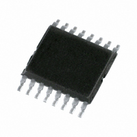
SC18IS602BIPW,112 NXP Semiconductors, SC18IS602BIPW,112 Datasheet - Page 12

SC18IS602BIPW,112
Manufacturer Part Number
SC18IS602BIPW,112
Description
IC BRIDGE SPI/I2C 16-TSSOP
Manufacturer
NXP Semiconductors
Specifications of SC18IS602BIPW,112
Controller Type
I²C Bus Controller
Interface
I²C
Voltage - Supply
2.4 V ~ 3.6 V
Current - Supply
11mA
Operating Temperature
-40°C ~ 85°C
Mounting Type
Surface Mount
Package / Case
16-TSSOP
Operating Temperature Classification
Military
Operating Temperature (max)
125C
Package Type
TSSOP
Rad Hardened
No
Maximum Operating Frequency
4.5 MHz
Maximum Operating Temperature
+ 125 C
Minimum Operating Temperature
- 55 C
Mounting Style
SMD/SMT
Supply Voltage (max)
3.6 V
Supply Voltage (min)
2.4 V
For Use With
568-4705 - DEMO BOARD I2C TO SPI SC18IS602
Lead Free Status / RoHS Status
Lead free / RoHS Compliant
Other names
568-4785-5
935286182112
SC18IS602BIPW
SC18IS602BIPW,112
SC18IS602BIPW
935286182112
SC18IS602BIPW
SC18IS602BIPW,112
SC18IS602BIPW
Available stocks
Company
Part Number
Manufacturer
Quantity
Price
Company:
Part Number:
SC18IS602BIPW,112
Manufacturer:
NXP
Quantity:
463
NXP Semiconductors
SC18IS602_602B_603_4
Product data sheet
7.1.11.3 Input-only configuration
7.1.11.4 Push-pull output configuration
The input-only pin configuration is shown in
also has a glitch suppression circuit.
The push-pull output configuration has the same pull-down structure as both the
open-drain and the quasi-bidirectional output modes but provides a continuous strong
pull-up when the port latch contains a logic 1. The push-pull mode may be used when
more source current is needed from a pin output.
The push-pull pin configuration is shown in
A push-pull pin has a Schmitt-triggered input that also has a glitch suppression circuit.
Fig 17. Open-drain output configuration
Fig 18. Input-only configuration
Fig 19. Push-pull output configuration
pin latch data
pin latch data
Rev. 04 — 11 March 2008
input data
input data
input data
V
SS
Figure
Figure
glitch rejection
N
P
SC18IS602/602B/603
V
SS
glitch rejection
strong
19.
18. It is a Schmitt-triggered input that
V
DD
glitch rejection
002aab884
GPIO pin
002aab885
GPIO pin
I
002aab883
GPIO pin
2
C-bus to SPI bridge
© NXP B.V. 2008. All rights reserved.
12 of 25


