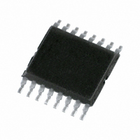
SC18IS602BIPW,112 NXP Semiconductors, SC18IS602BIPW,112 Datasheet - Page 3

SC18IS602BIPW,112
Manufacturer Part Number
SC18IS602BIPW,112
Description
IC BRIDGE SPI/I2C 16-TSSOP
Manufacturer
NXP Semiconductors
Specifications of SC18IS602BIPW,112
Controller Type
I²C Bus Controller
Interface
I²C
Voltage - Supply
2.4 V ~ 3.6 V
Current - Supply
11mA
Operating Temperature
-40°C ~ 85°C
Mounting Type
Surface Mount
Package / Case
16-TSSOP
Operating Temperature Classification
Military
Operating Temperature (max)
125C
Package Type
TSSOP
Rad Hardened
No
Maximum Operating Frequency
4.5 MHz
Maximum Operating Temperature
+ 125 C
Minimum Operating Temperature
- 55 C
Mounting Style
SMD/SMT
Supply Voltage (max)
3.6 V
Supply Voltage (min)
2.4 V
For Use With
568-4705 - DEMO BOARD I2C TO SPI SC18IS602
Lead Free Status / RoHS Status
Lead free / RoHS Compliant
Other names
568-4785-5
935286182112
SC18IS602BIPW
SC18IS602BIPW,112
SC18IS602BIPW
935286182112
SC18IS602BIPW
SC18IS602BIPW,112
SC18IS602BIPW
Available stocks
Company
Part Number
Manufacturer
Quantity
Price
Company:
Part Number:
SC18IS602BIPW,112
Manufacturer:
NXP
Quantity:
463
NXP Semiconductors
6. Pinning information
Table 2.
[1]
[2]
SC18IS602_602B_603_4
Product data sheet
Symbol
SS0/GPIO0
SS1/GPIO1
RESET
V
MISO
MOSI
SDA
SCL
INT
SS2/GPIO2
SPICLK
V
SS3/GPIO3
CLKIN
A0
A1
A2
Fig 3.
SS
DD
SC18IS602IPW and SC18IS603IPW do not support SS2. This pin should be used as GPIO2 only.
SC18IS602BIPW does support SS2/GPIO2 function. This pin can be used as SS2 or GPIO2.
SS0/GPIO0
SS1/GPIO1
a. SC18IS602/602B
RESET
Pin configuration for TSSOP16
MISO
MOSI
Pin description
SDA
SCL
V
SS
Pin
SC18IS602,
SC18IS602B
1
2
3
4
5
6
7
8
9
10
11
12
13
-
14
15
16
1
2
3
4
5
6
7
8
6.1 Pinning
6.2 Pin description
[1][2]
SC18IS602BIPW
SC18IS602IPW
SC18IS603
1
2
3
4
5
6
7
8
9
10
11
12
-
13
14
15
16
002aac441
[1]
16
15
14
13
12
11
10
9
A2
A1
A0
SS3/GPIO3
V
SPICLK
SS2/GPIO2
INT
DD
Type
I/O
I/O
I
-
I
O
I/O
I
O
I/O
O
-
I/O
I
I
I
I
Rev. 04 — 11 March 2008
Description
SPI slave select output 0 (active LOW) or GPIO 0
SPI slave select output 1 (active LOW) or GPIO 1
reset input (active LOW)
ground supply
Master In, Slave Out
Master Out, Slave In
I
I
interrupt output (active LOW)
SPI slave select output 2 (active LOW) or GPIO 2
SPI clock
supply voltage
SPI slave select output 3 (active LOW) or GPIO 3
external clock input
address input 0
address input 1
address input 2
2
2
C-bus data
C-bus clock
SS0/GPIO0
SS1/GPIO1
b. SC18IS603
RESET
MISO
MOSI
SDA
SCL
V
SC18IS602/602B/603
SS
1
2
3
4
5
6
7
8
SC18IS603IPW
002aac442
I
2
C-bus to SPI bridge
© NXP B.V. 2008. All rights reserved.
16
15
14
13
12
11
10
9
A2
A1
A0
CLKIN
V
SPICLK
SS2/GPIO2
INT
DD
3 of 25


