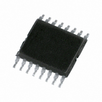
SC18IS602BIPW,112 NXP Semiconductors, SC18IS602BIPW,112 Datasheet - Page 5

SC18IS602BIPW,112
Manufacturer Part Number
SC18IS602BIPW,112
Description
IC BRIDGE SPI/I2C 16-TSSOP
Manufacturer
NXP Semiconductors
Specifications of SC18IS602BIPW,112
Controller Type
I²C Bus Controller
Interface
I²C
Voltage - Supply
2.4 V ~ 3.6 V
Current - Supply
11mA
Operating Temperature
-40°C ~ 85°C
Mounting Type
Surface Mount
Package / Case
16-TSSOP
Operating Temperature Classification
Military
Operating Temperature (max)
125C
Package Type
TSSOP
Rad Hardened
No
Maximum Operating Frequency
4.5 MHz
Maximum Operating Temperature
+ 125 C
Minimum Operating Temperature
- 55 C
Mounting Style
SMD/SMT
Supply Voltage (max)
3.6 V
Supply Voltage (min)
2.4 V
For Use With
568-4705 - DEMO BOARD I2C TO SPI SC18IS602
Lead Free Status / RoHS Status
Lead free / RoHS Compliant
Other names
568-4785-5
935286182112
SC18IS602BIPW
SC18IS602BIPW,112
SC18IS602BIPW
935286182112
SC18IS602BIPW
SC18IS602BIPW,112
SC18IS602BIPW
Available stocks
Company
Part Number
Manufacturer
Quantity
Price
Company:
Part Number:
SC18IS602BIPW,112
Manufacturer:
NXP
Quantity:
463
NXP Semiconductors
SC18IS602_602B_603_4
Product data sheet
7.1.1 Addressing
7.1.2 Write to data buffer
7.1.3 SPI read and write - Function ID 01h to 0Fh
The first seven bits of the first byte sent after a START condition defines the slave address
of the device being accessed on the bus. The eighth bit determines the direction of the
message. A ‘0’ in the least significant position of the first byte means that the master will
write information to a selected slave. A ‘1’ in this position means that the master will read
information from the slave. When an address is sent, each device in a system compares
the first seven bits after the START condition with its address. If they match, the device
considers itself addressed by the master as a slave-receiver or slave-transmitter,
depending on the R/W bit.
A slave address of the SC18IS602/602B/603 is comprised of a fixed and a programmable
part. The programmable part of the slave address enables the maximum possible number
of such devices to be connected to the I
three programmable address bits (defined by the A2, A1, and A0 pins), it is possible to
have eight of these devices on the same bus.
The state of the A2, A1, and A0 pins are latched at reset. Changes made after reset will
not alter the address.
All communications to or from the SC18IS602/602B/603 occur through the data buffer.
The data buffer is 200 bytes deep. A message begins with the SC18IS60x address,
followed by the Function ID. Depending upon the Function ID, zero to 200 data bytes can
follow.
The SC18IS60x will place the data received into a buffer and continue loading the buffer
until a STOP condition is received. After the STOP condition is detected, further
communications will not be acknowledged until the function designated by the Function ID
has been completed.
Data in the buffer will be sent to the SPI port if the Function ID is 01h to 0Fh. The Function
ID contains the Slave Select (SS) to be used for the transmission on the SPI port. There
are four Slave Selects that can be used, with each SS being selected by one of the bits in
Fig 5.
Fig 6.
Slave address
Write to data buffer
S
SLAVE ADDRESS
Rev. 04 — 11 March 2008
0
W
1
A
fixed
slave address
0
FUNCTION ID
2
C-bus. Since the SC18IS602/602B/603 have
1
programmable
SC18IS602/602B/603
A2
A1
A0
002aac446
A
R/W
X
0 TO 200 BYTES
I
2
C-bus to SPI bridge
002aac447
© NXP B.V. 2008. All rights reserved.
A
P
5 of 25


