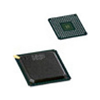
PNX1500E NXP Semiconductors, PNX1500E Datasheet - Page 103

PNX1500E
Manufacturer Part Number
PNX1500E
Description
Manufacturer
NXP Semiconductors
Datasheet
1.PNX1500E.pdf
(828 pages)
Specifications of PNX1500E
Lead Free Status / Rohs Status
Not Compliant
Available stocks
Company
Part Number
Manufacturer
Quantity
Price
Company:
Part Number:
PNX1500E
Manufacturer:
NORTEL
Quantity:
1 000
- Current page: 103 of 828
- Download datasheet (4Mb)
NXP Semiconductors
Volume 1 of 1
PNX15XX_PNX952X_SER_N_4
Product data sheet
10.3.1 PCI Capabilities
10.2 IR Remote Control Receiver and Blaster
10.3 PCI-2.2 & XIO-16 Bus Interface Unit
This allows use of GPIO for a variety of functions.
PNX15xx/952x Series uses the GPIO pin event sequence timestamping mechanism
and software to interpret remote control commands. The event sequence
timestamping can resolve events on signal edges with 75 ns accuracy. A sequence of
events followed by a period of inactivity causes generation of an interrupt. Software
then interprets the ‘character’ by looking at the event list consisting of (time, direction)
encoded in memory.
This allows interpretation of a wide variety of Remote Control protocols. The NXP
RC-5, RC-6 and RC-MM remote control protocols are all decoded with this
mechanism, provided that the RF demodulation is performed externally. Most other
Consumer Electronic vendor remote control protocols can be supported by
appropriate software.
Similarly, the event generation mechanism can be used to implement IR blaster
capability. In this case, the modulator is included - the software generated pulses can
be superimposed on an internally generated carrier.
There are some speed considerations with this mechanism. Each character
communicated generates at least one interrupt, and possibly more if the number of
edge events exceeds the FIFO size. Hence, this mechanism is suitable only for
protocols that use frequencies up to a few 10’s of kHz, with low character repetition
rates, and not for high speed protocols.
PNX15xx/952x Series contains an expansion bus interface unit ‘PCI/XIO-16’ that
allows easy connection of a variety of board level memory components and
peripherals. The bus interface is a single set of pins that allows simultaneous
connection of 32-bit PCI master/slave devices as well as separated address/data
style 8- and 16-bit micro processor slave peripherals and standard (NOR) or disk-
type (NAND) Flash memory.
The bus interface unit contains a built-in single-channel DMA unit that can move
blocks of data to or from an external peripheral (PCI bus master or slave) to or from
PNX15xx/952x Series DRAM. The DMA unit can access PCI as well as 8- and 16-bit
wide XIO devices. The DMA unit packs XIO device data to/from 32-bit words, so that
no CPU involvement is required to pre/post process data.
PNX15xx/952x Series complies with Revision 2.2 of the PCI bus specification, and
operates as a 32-bit PCI master/target up to 33 MHz.
•
•
50% of the pins will have a ‘low’ reset value
50% have a ‘high’ reset value
Rev. 4.0 — 03 December 2007
PNX15xx/952x Series
Chapter 2: Overview
© NXP B.V. 2007. All rights reserved.
2-103
Related parts for PNX1500E
Image
Part Number
Description
Manufacturer
Datasheet
Request
R
Part Number:
Description:
NXP Semiconductors designed the LPC2420/2460 microcontroller around a 16-bit/32-bitARM7TDMI-S CPU core with real-time debug interfaces that include both JTAG andembedded trace
Manufacturer:
NXP Semiconductors
Datasheet:

Part Number:
Description:
NXP Semiconductors designed the LPC2458 microcontroller around a 16-bit/32-bitARM7TDMI-S CPU core with real-time debug interfaces that include both JTAG andembedded trace
Manufacturer:
NXP Semiconductors
Datasheet:
Part Number:
Description:
NXP Semiconductors designed the LPC2468 microcontroller around a 16-bit/32-bitARM7TDMI-S CPU core with real-time debug interfaces that include both JTAG andembedded trace
Manufacturer:
NXP Semiconductors
Datasheet:
Part Number:
Description:
NXP Semiconductors designed the LPC2470 microcontroller, powered by theARM7TDMI-S core, to be a highly integrated microcontroller for a wide range ofapplications that require advanced communications and high quality graphic displays
Manufacturer:
NXP Semiconductors
Datasheet:
Part Number:
Description:
NXP Semiconductors designed the LPC2478 microcontroller, powered by theARM7TDMI-S core, to be a highly integrated microcontroller for a wide range ofapplications that require advanced communications and high quality graphic displays
Manufacturer:
NXP Semiconductors
Datasheet:
Part Number:
Description:
The Philips Semiconductors XA (eXtended Architecture) family of 16-bit single-chip microcontrollers is powerful enough to easily handle the requirements of high performance embedded applications, yet inexpensive enough to compete in the market for hi
Manufacturer:
NXP Semiconductors
Datasheet:
Part Number:
Description:
The XA-S3 device is a member of Philips Semiconductors? XA(eXtended Architecture) family of high performance 16-bitsingle-chip microcontrollers
Manufacturer:
NXP Semiconductors
Datasheet:

Part Number:
Description:
The NXP BlueStreak LH75401/LH75411 family consists of two low-cost 16/32-bit System-on-Chip (SoC) devices
Manufacturer:
NXP Semiconductors
Datasheet:

Part Number:
Description:
The NXP LPC3130/3131 combine an 180 MHz ARM926EJ-S CPU core, high-speed USB2
Manufacturer:
NXP Semiconductors
Datasheet:

Part Number:
Description:
The NXP LPC3141 combine a 270 MHz ARM926EJ-S CPU core, High-speed USB 2
Manufacturer:
NXP Semiconductors

Part Number:
Description:
The NXP LPC3143 combine a 270 MHz ARM926EJ-S CPU core, High-speed USB 2
Manufacturer:
NXP Semiconductors

Part Number:
Description:
The NXP LPC3152 combines an 180 MHz ARM926EJ-S CPU core, High-speed USB 2
Manufacturer:
NXP Semiconductors

Part Number:
Description:
The NXP LPC3154 combines an 180 MHz ARM926EJ-S CPU core, High-speed USB 2
Manufacturer:
NXP Semiconductors

Part Number:
Description:
Standard level N-channel enhancement mode Field-Effect Transistor (FET) in a plastic package using NXP High-Performance Automotive (HPA) TrenchMOS technology
Manufacturer:
NXP Semiconductors
Datasheet:


