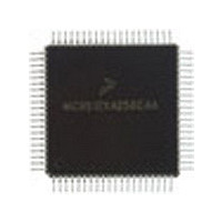
MC9S12C128VFU Freescale Semiconductor, MC9S12C128VFU Datasheet - Page 192

MC9S12C128VFU
Manufacturer Part Number
MC9S12C128VFU
Description
Manufacturer
Freescale Semiconductor
Datasheet
1.MC9S12C128VFU.pdf
(690 pages)
Specifications of MC9S12C128VFU
Cpu Family
HCS12
Device Core Size
16b
Frequency (max)
25MHz
Interface Type
CAN/SCI/SPI
Program Memory Type
Flash
Program Memory Size
128KB
Total Internal Ram Size
4KB
# I/os (max)
60
Number Of Timers - General Purpose
8
Operating Supply Voltage (typ)
2.5/5V
Operating Supply Voltage (max)
2.75/5.5V
Operating Supply Voltage (min)
2.35/2.97V
On-chip Adc
8-chx10-bit
Instruction Set Architecture
CISC
Operating Temp Range
-40C to 105C
Operating Temperature Classification
Industrial
Mounting
Surface Mount
Pin Count
80
Package Type
PQFP
Lead Free Status / Rohs Status
Not Compliant
Available stocks
Company
Part Number
Manufacturer
Quantity
Price
Company:
Part Number:
MC9S12C128VFUE
Manufacturer:
Freescale
Quantity:
38 000
Company:
Part Number:
MC9S12C128VFUE
Manufacturer:
Freescale Semiconductor
Quantity:
10 000
- Current page: 192 of 690
- Download datasheet (4Mb)
Chapter 7 Debug Module (DBGV1) Block Description
The DBG in DBG mode includes these distinctive features:
192
•
•
•
•
•
•
•
Three comparators (A, B, and C)
— Dual mode, comparators A and B used to compare addresses
— Full mode, comparator A compares address and comparator B compares data
— Can be used as trigger and/or breakpoint
— Comparator C used in LOOP1 capture mode or as additional breakpoint
Four capture modes
— Normal mode, change-of-flow information is captured based on trigger specification
— Loop1 mode, comparator C is dynamically updated to prevent redundant change-of-flow
— Detail mode, address and data for all cycles except program fetch (P) and free (f) cycles are
— Profile mode, last instruction address executed by CPU is returned when trace buffer address is
Two types of breakpoint or debug triggers
— Break just before a specific instruction will begin execution (tag)
— Break on the first instruction boundary after a match occurs (force)
BDM or SWI breakpoint
— Enter BDM on breakpoint (BDM)
— Execute SWI on breakpoint (SWI)
Nine trigger modes for comparators A and B
— A
— A or B
— A then B
— A and B, where B is data (full mode)
— A and not B, where B is data (full mode)
— Event only B, store data
— A then event only B, store data
— Inside range, A ≤ address ≤ B
— Outside range, address < Α or address > B
Comparator C provides an additional tag or force breakpoint when capture mode is not configured
in LOOP1 mode.
Sixty-four word (16 bits wide) trace buffer for storing change-of-flow information, event only data
and other bus information.
— Source address of taken conditional branches (long, short, bit-conditional, and loop constructs)
— Destination address of indexed JMP, JSR, and CALL instruction.
— Destination address of RTI, RTS, and RTC instructions
— Vector address of interrupts, except for SWI and BDM vectors
storage.
stored in trace buffer
read
MC9S12C-Family / MC9S12GC-Family
Rev 01.24
Freescale Semiconductor
Related parts for MC9S12C128VFU
Image
Part Number
Description
Manufacturer
Datasheet
Request
R
Part Number:
Description:
Manufacturer:
Freescale Semiconductor, Inc
Datasheet:
Part Number:
Description:
Manufacturer:
Freescale Semiconductor, Inc
Datasheet:
Part Number:
Description:
Manufacturer:
Freescale Semiconductor, Inc
Datasheet:
Part Number:
Description:
Manufacturer:
Freescale Semiconductor, Inc
Datasheet:
Part Number:
Description:
Manufacturer:
Freescale Semiconductor, Inc
Datasheet:
Part Number:
Description:
Manufacturer:
Freescale Semiconductor, Inc
Datasheet:
Part Number:
Description:
Manufacturer:
Freescale Semiconductor, Inc
Datasheet:
Part Number:
Description:
Manufacturer:
Freescale Semiconductor, Inc
Datasheet:
Part Number:
Description:
Manufacturer:
Freescale Semiconductor, Inc
Datasheet:
Part Number:
Description:
Manufacturer:
Freescale Semiconductor, Inc
Datasheet:
Part Number:
Description:
Manufacturer:
Freescale Semiconductor, Inc
Datasheet:
Part Number:
Description:
Manufacturer:
Freescale Semiconductor, Inc
Datasheet:
Part Number:
Description:
Manufacturer:
Freescale Semiconductor, Inc
Datasheet:
Part Number:
Description:
Manufacturer:
Freescale Semiconductor, Inc
Datasheet:
Part Number:
Description:
Manufacturer:
Freescale Semiconductor, Inc
Datasheet:


