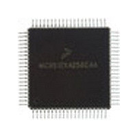
MC9S12C128VFU Freescale Semiconductor, MC9S12C128VFU Datasheet - Page 353

MC9S12C128VFU
Manufacturer Part Number
MC9S12C128VFU
Description
Manufacturer
Freescale Semiconductor
Datasheet
1.MC9S12C128VFU.pdf
(690 pages)
Specifications of MC9S12C128VFU
Cpu Family
HCS12
Device Core Size
16b
Frequency (max)
25MHz
Interface Type
CAN/SCI/SPI
Program Memory Type
Flash
Program Memory Size
128KB
Total Internal Ram Size
4KB
# I/os (max)
60
Number Of Timers - General Purpose
8
Operating Supply Voltage (typ)
2.5/5V
Operating Supply Voltage (max)
2.75/5.5V
Operating Supply Voltage (min)
2.35/2.97V
On-chip Adc
8-chx10-bit
Instruction Set Architecture
CISC
Operating Temp Range
-40C to 105C
Operating Temperature Classification
Industrial
Mounting
Surface Mount
Pin Count
80
Package Type
PQFP
Lead Free Status / Rohs Status
Not Compliant
Available stocks
Company
Part Number
Manufacturer
Quantity
Price
Company:
Part Number:
MC9S12C128VFUE
Manufacturer:
Freescale
Quantity:
38 000
Company:
Part Number:
MC9S12C128VFUE
Manufacturer:
Freescale Semiconductor
Quantity:
10 000
- Current page: 353 of 690
- Download datasheet (4Mb)
12.3.2.1
Each PWM channel has an enable bit (PWMEx) to start its waveform output. When any of the PWMEx
bits are set (PWMEx = 1), the associated PWM output is enabled immediately. However, the actual PWM
waveform is not available on the associated PWM output until its clock source begins its next cycle due to
the synchronization of PWMEx and the clock source.
An exception to this is when channels are concatenated. After concatenated mode is enabled (CONxx bits
set in PWMCTL register), enabling/disabling the corresponding 16-bit PWM channel is controlled by the
low-order PWMEx bit. In this case, the high-order bytes PWMEx bits have no effect and their
corresponding PWM output lines are disabled.
While in run mode, if all six PWM channels are disabled (PWME5–PWME0 = 0), the prescaler counter
shuts off for power savings.
Read: anytime
Write: anytime
Freescale Semiconductor
Module Base + 0x0000
PWME5
PWME4
PWME3
PWME2
Reset
Field
5
4
3
2
W
R
Pulse Width Channel 5 Enable
0 Pulse width channel 5 is disabled.
1 Pulse width channel 5 is enabled. The pulse modulated signal becomes available at PWM,output bit 5 when
Pulse Width Channel 4 Enable
0 Pulse width channel 4 is disabled.
1 Pulse width channel 4 is enabled. The pulse modulated signal becomes available at PWM, output bit 4 when
Pulse Width Channel 3 Enable
0 Pulse width channel 3 is disabled.
1 Pulse width channel 3 is enabled. The pulse modulated signal becomes available at PWM, output bit 3 when
Pulse Width Channel 2 Enable
0 Pulse width channel 2 is disabled.
1 Pulse width channel 2 is enabled. The pulse modulated signal becomes available at PWM, output bit 2 when
PWM Enable Register (PWME)
0
0
7
its clock source begins its next cycle.
its clock source begins its next cycle. If CON45 = 1, then bit has no effect and PWM output line 4 is disabled.
its clock source begins its next cycle.
its clock source begins its next cycle. If CON23 = 1, then bit has no effect and PWM output line 2 is disabled.
The first PWM cycle after enabling the channel can be irregular.
= Unimplemented or Reserved
0
0
6
Figure 12-3. PWM Enable Register (PWME)
Table 12-2. PWME Field Descriptions
PWME5
MC9S12C-Family / MC9S12GC-Family
0
5
PWME4
Rev 01.24
NOTE
0
4
Chapter 12 Pulse-Width Modulator (PWM8B6CV1) Block Description
Description
PWME3
0
3
PWME2
0
2
PWME1
0
1
PWME0
0
0
353
Related parts for MC9S12C128VFU
Image
Part Number
Description
Manufacturer
Datasheet
Request
R
Part Number:
Description:
Manufacturer:
Freescale Semiconductor, Inc
Datasheet:
Part Number:
Description:
Manufacturer:
Freescale Semiconductor, Inc
Datasheet:
Part Number:
Description:
Manufacturer:
Freescale Semiconductor, Inc
Datasheet:
Part Number:
Description:
Manufacturer:
Freescale Semiconductor, Inc
Datasheet:
Part Number:
Description:
Manufacturer:
Freescale Semiconductor, Inc
Datasheet:
Part Number:
Description:
Manufacturer:
Freescale Semiconductor, Inc
Datasheet:
Part Number:
Description:
Manufacturer:
Freescale Semiconductor, Inc
Datasheet:
Part Number:
Description:
Manufacturer:
Freescale Semiconductor, Inc
Datasheet:
Part Number:
Description:
Manufacturer:
Freescale Semiconductor, Inc
Datasheet:
Part Number:
Description:
Manufacturer:
Freescale Semiconductor, Inc
Datasheet:
Part Number:
Description:
Manufacturer:
Freescale Semiconductor, Inc
Datasheet:
Part Number:
Description:
Manufacturer:
Freescale Semiconductor, Inc
Datasheet:
Part Number:
Description:
Manufacturer:
Freescale Semiconductor, Inc
Datasheet:
Part Number:
Description:
Manufacturer:
Freescale Semiconductor, Inc
Datasheet:
Part Number:
Description:
Manufacturer:
Freescale Semiconductor, Inc
Datasheet:


