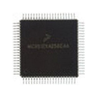
MC9S12C128VFU Freescale Semiconductor, MC9S12C128VFU Datasheet - Page 241

MC9S12C128VFU
Manufacturer Part Number
MC9S12C128VFU
Description
Manufacturer
Freescale Semiconductor
Datasheet
1.MC9S12C128VFU.pdf
(690 pages)
Specifications of MC9S12C128VFU
Cpu Family
HCS12
Device Core Size
16b
Frequency (max)
25MHz
Interface Type
CAN/SCI/SPI
Program Memory Type
Flash
Program Memory Size
128KB
Total Internal Ram Size
4KB
# I/os (max)
60
Number Of Timers - General Purpose
8
Operating Supply Voltage (typ)
2.5/5V
Operating Supply Voltage (max)
2.75/5.5V
Operating Supply Voltage (min)
2.35/2.97V
On-chip Adc
8-chx10-bit
Instruction Set Architecture
CISC
Operating Temp Range
-40C to 105C
Operating Temperature Classification
Industrial
Mounting
Surface Mount
Pin Count
80
Package Type
PQFP
Lead Free Status / Rohs Status
Not Compliant
Available stocks
Company
Part Number
Manufacturer
Quantity
Price
Company:
Part Number:
MC9S12C128VFUE
Manufacturer:
Freescale
Quantity:
38 000
Company:
Part Number:
MC9S12C128VFUE
Manufacturer:
Freescale Semiconductor
Quantity:
10 000
- Current page: 241 of 690
- Download datasheet (4Mb)
8.3.2.10
This read-only register contains the Conversion Complete Flags.
Read: Anytime
Write: Anytime, no effect
Freescale Semiconductor
Module Base + 0x000B
CCF[7:0]
Reset
Field
7–0
W
R
CCF7
Conversion Complete Flag x (x = 7, 6, 5, 4, 3, 2, 1, 0) — A conversion complete flag is set at the end of each
conversion in a conversion sequence. The flags are associated with the conversion position in a sequence (and
also the result register number). Therefore, CCF0 is set when the first conversion in a sequence is complete and
the result is available in result register ATDDR0; CCF1 is set when the second conversion in a sequence is
complete and the result is available in ATDDR1, and so forth. A flag CCFx (x = 7, 6, 5, 4, 3, 2, 1, 0) is cleared
when one of the following occurs:
0 Conversion number x not completed
1 Conversion number x has completed, result ready in ATDDRx
ATD Status Register 1 (ATDSTAT1)
0
7
A) Write to ATDCTL5 (a new conversion sequence is started)
B) If AFFC = 0 and read of ATDSTAT1 followed by read of result register ATDDRx
C) If AFFC = 1 and read of result register ATDDRx
= Unimplemented or Reserved
CCF6
0
6
Figure 8-12. ATD Status Register 1 (ATDSTAT1)
Table 8-16. ATDSTAT1 Field Descriptions
CCF5
MC9S12C-Family / MC9S12GC-Family
0
5
CCF4
Rev 01.24
0
4
Chapter 8 Analog-to-Digital Converter (ATD10B8C) Block Description
Description
CCF3
0
3
CCF2
0
2
CCF1
0
1
CCF0
0
0
241
Related parts for MC9S12C128VFU
Image
Part Number
Description
Manufacturer
Datasheet
Request
R
Part Number:
Description:
Manufacturer:
Freescale Semiconductor, Inc
Datasheet:
Part Number:
Description:
Manufacturer:
Freescale Semiconductor, Inc
Datasheet:
Part Number:
Description:
Manufacturer:
Freescale Semiconductor, Inc
Datasheet:
Part Number:
Description:
Manufacturer:
Freescale Semiconductor, Inc
Datasheet:
Part Number:
Description:
Manufacturer:
Freescale Semiconductor, Inc
Datasheet:
Part Number:
Description:
Manufacturer:
Freescale Semiconductor, Inc
Datasheet:
Part Number:
Description:
Manufacturer:
Freescale Semiconductor, Inc
Datasheet:
Part Number:
Description:
Manufacturer:
Freescale Semiconductor, Inc
Datasheet:
Part Number:
Description:
Manufacturer:
Freescale Semiconductor, Inc
Datasheet:
Part Number:
Description:
Manufacturer:
Freescale Semiconductor, Inc
Datasheet:
Part Number:
Description:
Manufacturer:
Freescale Semiconductor, Inc
Datasheet:
Part Number:
Description:
Manufacturer:
Freescale Semiconductor, Inc
Datasheet:
Part Number:
Description:
Manufacturer:
Freescale Semiconductor, Inc
Datasheet:
Part Number:
Description:
Manufacturer:
Freescale Semiconductor, Inc
Datasheet:
Part Number:
Description:
Manufacturer:
Freescale Semiconductor, Inc
Datasheet:


