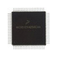
MC9S12C128VFU Freescale Semiconductor, MC9S12C128VFU Datasheet - Page 486

MC9S12C128VFU
Manufacturer Part Number
MC9S12C128VFU
Description
Manufacturer
Freescale Semiconductor
Datasheet
1.MC9S12C128VFU.pdf
(690 pages)
Specifications of MC9S12C128VFU
Cpu Family
HCS12
Device Core Size
16b
Frequency (max)
25MHz
Interface Type
CAN/SCI/SPI
Program Memory Type
Flash
Program Memory Size
128KB
Total Internal Ram Size
4KB
# I/os (max)
60
Number Of Timers - General Purpose
8
Operating Supply Voltage (typ)
2.5/5V
Operating Supply Voltage (max)
2.75/5.5V
Operating Supply Voltage (min)
2.35/2.97V
On-chip Adc
8-chx10-bit
Instruction Set Architecture
CISC
Operating Temp Range
-40C to 105C
Operating Temperature Classification
Industrial
Mounting
Surface Mount
Pin Count
80
Package Type
PQFP
Lead Free Status / Rohs Status
Not Compliant
Available stocks
Company
Part Number
Manufacturer
Quantity
Price
Company:
Part Number:
MC9S12C128VFUE
Manufacturer:
Freescale
Quantity:
38 000
Company:
Part Number:
MC9S12C128VFUE
Manufacturer:
Freescale Semiconductor
Quantity:
10 000
- Current page: 486 of 690
- Download datasheet (4Mb)
Chapter 17 16 Kbyte Flash Module (S12FTS16KV1)
All bits read 0 and are not writable.
17.4
17.4.1
Write operations are used for the program, erase, and erase verify algorithms described in this section. The
program and erase algorithms are controlled by a state machine whose timebase FCLK is derived from the
oscillator clock via a programmable divider. The FCMD register as well as the associated FADDR and
FDATA registers operate as a buffer and a register (2-stage FIFO) so that a new command along with the
necessary data and address can be stored to the buffer while the previous command is still in progress. This
pipelined operation allows a time optimization when programming more than one word on a specific row,
as the high voltage generation can be kept active in between two programming commands. The pipelined
operation also allows a simplification of command launching. Buffer empty as well as command
completion are signalled by flags in the FSTAT register with corresponding interrupts generated, if
enabled.
The next sections describe:
17.4.1.1
Prior to issuing any Flash command after a reset, it is first necessary to write the FCLKDIV register to
divide the oscillator clock down to within the 150-kHz to 200-kHz range. Since the program and erase
timings are also a function of the bus clock, the FCLKDIV determination must take this information into
account.
If we define:
486
Module Base + 0x000F
Reset
•
•
•
•
•
•
•
W
R
How to write the FCLKDIV register
Command write sequence used to program, erase or erase verify the Flash array
Valid Flash commands
Errors resulting from illegal Flash operations
FCLK as the clock of the Flash timing control block
Tbus as the period of the bus clock
INT(x) as taking the integer part of x (e.g., INT(4.323) = 4),
Functional Description
Flash Command Operations
Writing the FCLKDIV Register
0
0
7
= Unimplemented or Reserved
0
0
6
MC9S12C-Family / MC9S12GC-Family
0
0
5
Figure 17-20. RESERVED6
Rev 01.24
0
0
4
0
0
3
0
0
2
Freescale Semiconductor
0
0
1
0
0
0
Related parts for MC9S12C128VFU
Image
Part Number
Description
Manufacturer
Datasheet
Request
R
Part Number:
Description:
Manufacturer:
Freescale Semiconductor, Inc
Datasheet:
Part Number:
Description:
Manufacturer:
Freescale Semiconductor, Inc
Datasheet:
Part Number:
Description:
Manufacturer:
Freescale Semiconductor, Inc
Datasheet:
Part Number:
Description:
Manufacturer:
Freescale Semiconductor, Inc
Datasheet:
Part Number:
Description:
Manufacturer:
Freescale Semiconductor, Inc
Datasheet:
Part Number:
Description:
Manufacturer:
Freescale Semiconductor, Inc
Datasheet:
Part Number:
Description:
Manufacturer:
Freescale Semiconductor, Inc
Datasheet:
Part Number:
Description:
Manufacturer:
Freescale Semiconductor, Inc
Datasheet:
Part Number:
Description:
Manufacturer:
Freescale Semiconductor, Inc
Datasheet:
Part Number:
Description:
Manufacturer:
Freescale Semiconductor, Inc
Datasheet:
Part Number:
Description:
Manufacturer:
Freescale Semiconductor, Inc
Datasheet:
Part Number:
Description:
Manufacturer:
Freescale Semiconductor, Inc
Datasheet:
Part Number:
Description:
Manufacturer:
Freescale Semiconductor, Inc
Datasheet:
Part Number:
Description:
Manufacturer:
Freescale Semiconductor, Inc
Datasheet:
Part Number:
Description:
Manufacturer:
Freescale Semiconductor, Inc
Datasheet:


