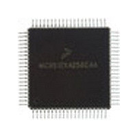
MC9S12C128VFU Freescale Semiconductor, MC9S12C128VFU Datasheet - Page 333

MC9S12C128VFU
Manufacturer Part Number
MC9S12C128VFU
Description
Manufacturer
Freescale Semiconductor
Datasheet
1.MC9S12C128VFU.pdf
(690 pages)
Specifications of MC9S12C128VFU
Cpu Family
HCS12
Device Core Size
16b
Frequency (max)
25MHz
Interface Type
CAN/SCI/SPI
Program Memory Type
Flash
Program Memory Size
128KB
Total Internal Ram Size
4KB
# I/os (max)
60
Number Of Timers - General Purpose
8
Operating Supply Voltage (typ)
2.5/5V
Operating Supply Voltage (max)
2.75/5.5V
Operating Supply Voltage (min)
2.35/2.97V
On-chip Adc
8-chx10-bit
Instruction Set Architecture
CISC
Operating Temp Range
-40C to 105C
Operating Temperature Classification
Industrial
Mounting
Surface Mount
Pin Count
80
Package Type
PQFP
Lead Free Status / Rohs Status
Not Compliant
Available stocks
Company
Part Number
Manufacturer
Quantity
Price
Company:
Part Number:
MC9S12C128VFUE
Manufacturer:
Freescale
Quantity:
38 000
Company:
Part Number:
MC9S12C128VFUE
Manufacturer:
Freescale Semiconductor
Quantity:
10 000
- Current page: 333 of 690
- Download datasheet (4Mb)
The synchronization jump width (see the Bosch CAN specification for details) can be programmed in a
range of 1 to 4 time quanta by setting the SJW parameter.
The SYNC_SEG, TSEG1, TSEG2, and SJW parameters are set by programming the MSCAN bus timing
registers (CANBTR0, CANBTR1) (see
and
Table 10-34
10.4.4
10.4.4.1
The MSCAN module behaves as described within this specification in all normal system operation modes.
10.4.4.2
The MSCAN module behaves as described within this specification in all special system operation modes.
Freescale Semiconductor
Section 10.3.2.4, “MSCAN Bus Timing Register 1
Time Segment 1
Modes of Operation
gives an overview of the CAN compliant segment settings and the related parameter values.
Normal Modes
Special Modes
5 .. 10
4 .. 11
5 .. 12
6 .. 13
7 .. 14
8 .. 15
9 .. 16
It is the user’s responsibility to ensure the bit time settings are in compliance
with the CAN standard.
Transmit Point
Sample Point
SYNC_SEG
Syntax
Table 10-34. CAN Standard Compliant Bit Time Segment Settings
TSEG1
3 .. 10
4 .. 11
5 .. 12
6 .. 13
7 .. 14
8 .. 15
4 .. 9
System expects transitions to occur on the CAN bus during this
period.
A node in transmit mode transfers a new value to the CAN bus at
this point.
A node in receive mode samples the CAN bus at this point. If the
three samples per bit option is selected, then this point marks the
position of the third sample.
Table 10-33. Time Segment Syntax
MC9S12C-Family / MC9S12GC-Family
Time Segment 2
Section 10.3.2.3, “MSCAN Bus Timing Register 0
2
3
4
5
6
7
8
Chapter 10 Freescale’s Scalable Controller Area Network (S12MSCANV2)
Rev 01.24
NOTE
(CANBTR1)”).
Description
TSEG2
1
2
3
4
5
6
7
Synchronization
Jump Width
1 .. 2
1 .. 3
1 .. 4
1 .. 4
1 .. 4
1 .. 4
1 .. 4
(CANBTR0)”
SJW
0 .. 1
0 .. 2
0 .. 3
0 .. 3
0 .. 3
0 .. 3
0 .. 3
333
Related parts for MC9S12C128VFU
Image
Part Number
Description
Manufacturer
Datasheet
Request
R
Part Number:
Description:
Manufacturer:
Freescale Semiconductor, Inc
Datasheet:
Part Number:
Description:
Manufacturer:
Freescale Semiconductor, Inc
Datasheet:
Part Number:
Description:
Manufacturer:
Freescale Semiconductor, Inc
Datasheet:
Part Number:
Description:
Manufacturer:
Freescale Semiconductor, Inc
Datasheet:
Part Number:
Description:
Manufacturer:
Freescale Semiconductor, Inc
Datasheet:
Part Number:
Description:
Manufacturer:
Freescale Semiconductor, Inc
Datasheet:
Part Number:
Description:
Manufacturer:
Freescale Semiconductor, Inc
Datasheet:
Part Number:
Description:
Manufacturer:
Freescale Semiconductor, Inc
Datasheet:
Part Number:
Description:
Manufacturer:
Freescale Semiconductor, Inc
Datasheet:
Part Number:
Description:
Manufacturer:
Freescale Semiconductor, Inc
Datasheet:
Part Number:
Description:
Manufacturer:
Freescale Semiconductor, Inc
Datasheet:
Part Number:
Description:
Manufacturer:
Freescale Semiconductor, Inc
Datasheet:
Part Number:
Description:
Manufacturer:
Freescale Semiconductor, Inc
Datasheet:
Part Number:
Description:
Manufacturer:
Freescale Semiconductor, Inc
Datasheet:
Part Number:
Description:
Manufacturer:
Freescale Semiconductor, Inc
Datasheet:


