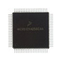
MC9S12C128VFU Freescale Semiconductor, MC9S12C128VFU Datasheet - Page 64

MC9S12C128VFU
Manufacturer Part Number
MC9S12C128VFU
Description
Manufacturer
Freescale Semiconductor
Datasheet
1.MC9S12C128VFU.pdf
(690 pages)
Specifications of MC9S12C128VFU
Cpu Family
HCS12
Device Core Size
16b
Frequency (max)
25MHz
Interface Type
CAN/SCI/SPI
Program Memory Type
Flash
Program Memory Size
128KB
Total Internal Ram Size
4KB
# I/os (max)
60
Number Of Timers - General Purpose
8
Operating Supply Voltage (typ)
2.5/5V
Operating Supply Voltage (max)
2.75/5.5V
Operating Supply Voltage (min)
2.35/2.97V
On-chip Adc
8-chx10-bit
Instruction Set Architecture
CISC
Operating Temp Range
-40C to 105C
Operating Temperature Classification
Industrial
Mounting
Surface Mount
Pin Count
80
Package Type
PQFP
Lead Free Status / Rohs Status
Not Compliant
Available stocks
Company
Part Number
Manufacturer
Quantity
Price
Company:
Part Number:
MC9S12C128VFUE
Manufacturer:
Freescale
Quantity:
38 000
Company:
Part Number:
MC9S12C128VFUE
Manufacturer:
Freescale Semiconductor
Quantity:
10 000
- Current page: 64 of 690
- Download datasheet (4Mb)
Chapter 1 MC9S12C and MC9S12GC Device Overview (MC9S12C128)
1.7.4
The VREGEN input mentioned in the VREG section is device internal, connected internally to V
1.7.5
In the 80-pin QFP package versions, both internal V
sides of the device as two pin pairs (V
internally. V
80-pin package to employ better supply routing and further decoupling.
1.7.6
The low voltage reset feature uses the low voltage reset signal from the VREG module as an input to the
CRG module. When the regulator output voltage supply to the internal chip logic falls below a specified
threshold the LVR signal from the VREG module causes the CRG module to generate a reset.
1.7.7
In the 48- and 52-pin package versions, the V
1.7.8
The MODRR register within the PIM allows for mapping of PWM channels to port T in the absence of
port P pins for the low pin count packages. For the 80QFP package option it is recommended not to use
MODRR since this is intended to support PWM channel availability in low pin count packages. Note that
when mapping PWM channels to port T in an 80QFP option, the associated PWM channels are then
mapped to both port P and port T. .
1.7.9
The port AD pins interface to the PIM module. However, the port pin digital state can be read from either
the PORTAD register in the ATD register map or from the PTAD register in the PIM register map.
In order to read a digital pin value from PORTAD the corresponding ATDDIEN bit must be set and the
corresponding DDRDA bit cleared. If the corresponding ATDDIEN bit is cleared then the pin is configured
as an analog input and the PORTAD bit reads back as "1".
In order to read a digital pin value from PTAD, the corresponding DDRAD bit must be cleared, to
configure the pin as an input.
Furthermore in order to use a port AD pin as an analog input, the corresponding DDRAD bit must be
cleared to configure the pin as an input
64
VREGEN
V
Clock Reset Generator And VREG Interface
Analog-to-Digital Converter
MODRR Register Port T And Port P Mapping
Port AD Dependency On PIM And ATD Registers
SS1
DD1
If the voltage regulator is shut down by connecting V
LVRF flag in the CRG flags register (CRGFLG) is undefined.
and V
, V
DD2
SS2
are connected together internally. The extra pin pair enables systems using the
, V
SS1
, V
MC9S12C-Family / MC9S12GC-Family
DD1
SS2
, V
SS1
RL
Rev 01.24
& V
pad is bonded internally to the V
NOTE
DD
DD2
and V
, V
SS2
SS
). V
of the 2.5V domain are bonded out on 2
DD1
DDR
and V
to ground then the
DD2
SSA
are connected together
Freescale Semiconductor
pin.
DDR
.
Related parts for MC9S12C128VFU
Image
Part Number
Description
Manufacturer
Datasheet
Request
R
Part Number:
Description:
Manufacturer:
Freescale Semiconductor, Inc
Datasheet:
Part Number:
Description:
Manufacturer:
Freescale Semiconductor, Inc
Datasheet:
Part Number:
Description:
Manufacturer:
Freescale Semiconductor, Inc
Datasheet:
Part Number:
Description:
Manufacturer:
Freescale Semiconductor, Inc
Datasheet:
Part Number:
Description:
Manufacturer:
Freescale Semiconductor, Inc
Datasheet:
Part Number:
Description:
Manufacturer:
Freescale Semiconductor, Inc
Datasheet:
Part Number:
Description:
Manufacturer:
Freescale Semiconductor, Inc
Datasheet:
Part Number:
Description:
Manufacturer:
Freescale Semiconductor, Inc
Datasheet:
Part Number:
Description:
Manufacturer:
Freescale Semiconductor, Inc
Datasheet:
Part Number:
Description:
Manufacturer:
Freescale Semiconductor, Inc
Datasheet:
Part Number:
Description:
Manufacturer:
Freescale Semiconductor, Inc
Datasheet:
Part Number:
Description:
Manufacturer:
Freescale Semiconductor, Inc
Datasheet:
Part Number:
Description:
Manufacturer:
Freescale Semiconductor, Inc
Datasheet:
Part Number:
Description:
Manufacturer:
Freescale Semiconductor, Inc
Datasheet:
Part Number:
Description:
Manufacturer:
Freescale Semiconductor, Inc
Datasheet:


