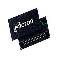
MT47H128M8HQ-3 L:G Micron Technology Inc, MT47H128M8HQ-3 L:G Datasheet - Page 105

MT47H128M8HQ-3 L:G
Manufacturer Part Number
MT47H128M8HQ-3 L:G
Description
IC DDR2 SDRAM 1GBIT 3NS 60FBGA
Manufacturer
Micron Technology Inc
Type
DDR2 SDRAMr
Specifications of MT47H128M8HQ-3 L:G
Format - Memory
RAM
Memory Type
DDR2 SDRAM
Memory Size
1G (128M x 8)
Speed
3ns
Interface
Parallel
Voltage - Supply
1.7 V ~ 1.9 V
Operating Temperature
0°C ~ 85°C
Package / Case
60-FBGA
Organization
128Mx8
Density
1Gb
Address Bus
17b
Access Time (max)
450ps
Maximum Clock Rate
667MHz
Operating Supply Voltage (typ)
1.8V
Package Type
FBGA
Operating Temp Range
0C to 85C
Operating Supply Voltage (max)
1.9V
Operating Supply Voltage (min)
1.7V
Supply Current
135mA
Pin Count
60
Mounting
Surface Mount
Operating Temperature Classification
Commercial
Lead Free Status / RoHS Status
Lead free / RoHS Compliant
- Current page: 105 of 131
- Download datasheet (10Mb)
Figure 60: WRITE Interrupted by WRITE
PDF: 09005aef821ae8bf
1GbDDR2.pdf – Rev. T 02/10 EN
DQS, DQS#
Command
Address
CK#
A10
DQ
CK
WRITE 1 a
Valid 5
T0
2-clock requirement
Notes:
NOP 2
T1
WL = 3
1. BL = 8 required and auto precharge must be disabled (A10 = LOW).
2. The NOP or COMMAND INHIBIT commands are valid. The PRECHARGE command cannot
3. The interrupting WRITE command must be issued exactly 2 ×
4. The earliest WRITE-to-PRECHARGE timing for WRITE at T0 is WL + BL/2 +
5. The WRITE command can be issued to any valid bank and row address (WRITE command
6. Auto precharge can be either enabled (A10 = HIGH) or disabled (A10 = LOW) by the in-
7. Subsequent rising DQS signals must align to the clock within
8. Example shown uses AL = 0; CL = 4, BL = 8.
be issued to banks used for WRITEs at T0 and T2.
starts with T7 and not T5 (because BL = 8 from MR and not the truncated length).
at T0 and T2 can be either same bank or different bank).
terrupting WRITE command.
WRITE 3 b
Valid 6
Valid 5
T2
NOP 2
T3
DI
a
WL = 3
a + 1
DI
NOP 2
a + 2
T4
7
DI
105
a + 3
DI
NOP 2
T5
DI
b
7
Micron Technology, Inc. reserves the right to change products or specifications without notice.
b + 1
DI
1Gb: x4, x8, x16 DDR2 SDRAM
NOP 2
b + 2
T6
DI
7
b + 3
DI
Valid 4
b + 4
T7
DI
7
Transitioning Data
© 2004 Micron Technology, Inc. All rights reserved.
t
t
b + 5
DQSS.
CK from previous WRITE.
DI
Valid 4
b + 6
T8
DI
7
b + 7
t
DI
WR where
Valid 4
Don’t Care
T9
WRITE
t
WR
Related parts for MT47H128M8HQ-3 L:G
Image
Part Number
Description
Manufacturer
Datasheet
Request
R

Part Number:
Description:
IC SDRAM 64MBIT 133MHZ 54TSOP
Manufacturer:
Micron Technology Inc
Datasheet:

Part Number:
Description:
IC SDRAM 64MBIT 5.5NS 86TSOP
Manufacturer:
Micron Technology Inc
Datasheet:

Part Number:
Description:
IC SDRAM 64MBIT 200MHZ 86TSOP
Manufacturer:
Micron Technology Inc
Datasheet:

Part Number:
Description:
IC SDRAM 64MBIT 133MHZ 54TSOP
Manufacturer:
Micron Technology Inc
Datasheet:

Part Number:
Description:
IC SDRAM 128MBIT 133MHZ 54TSOP
Manufacturer:
Micron Technology Inc
Datasheet:

Part Number:
Description:
IC SDRAM 256MBIT 133MHZ 90VFBGA
Manufacturer:
Micron Technology Inc
Datasheet:

Part Number:
Description:
IC SDRAM 128MBIT 133MHZ 54TSOP
Manufacturer:
Micron Technology Inc
Datasheet:

Part Number:
Description:
IC SDRAM 256MBIT 133MHZ 54TSOP
Manufacturer:
Micron Technology Inc
Datasheet:

Part Number:
Description:
IC DDR SDRAM 512MBIT 6NS 66TSOP
Manufacturer:
Micron Technology Inc
Datasheet:

Part Number:
Description:
IC SDRAM 128MBIT 167MHZ 86TSOP
Manufacturer:
Micron Technology Inc
Datasheet:

Part Number:
Description:
IC SDRAM 128MBIT 143MHZ 86TSOP
Manufacturer:
Micron Technology Inc
Datasheet:

Part Number:
Description:
SDRAM 256M-BIT 1.8V 54-PIN VFBGA
Manufacturer:
Micron Technology Inc
Datasheet:

Part Number:
Description:
IC SDRAM 128MBIT 143MHZ 86TSOP
Manufacturer:
Micron Technology Inc
Datasheet:

Part Number:
Description:
IC SDRAM 128MBIT 125MHZ 54VFBGA
Manufacturer:
Micron Technology Inc
Datasheet:

Part Number:
Description:
IC SDRAM 128MBIT 125MHZ 54VFBGA
Manufacturer:
Micron Technology Inc
Datasheet:


