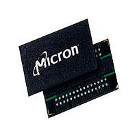
MT47H128M8HQ-3 L:G Micron Technology Inc, MT47H128M8HQ-3 L:G Datasheet - Page 86

MT47H128M8HQ-3 L:G
Manufacturer Part Number
MT47H128M8HQ-3 L:G
Description
IC DDR2 SDRAM 1GBIT 3NS 60FBGA
Manufacturer
Micron Technology Inc
Type
DDR2 SDRAMr
Specifications of MT47H128M8HQ-3 L:G
Format - Memory
RAM
Memory Type
DDR2 SDRAM
Memory Size
1G (128M x 8)
Speed
3ns
Interface
Parallel
Voltage - Supply
1.7 V ~ 1.9 V
Operating Temperature
0°C ~ 85°C
Package / Case
60-FBGA
Organization
128Mx8
Density
1Gb
Address Bus
17b
Access Time (max)
450ps
Maximum Clock Rate
667MHz
Operating Supply Voltage (typ)
1.8V
Package Type
FBGA
Operating Temp Range
0C to 85C
Operating Supply Voltage (max)
1.9V
Operating Supply Voltage (min)
1.7V
Supply Current
135mA
Pin Count
60
Mounting
Surface Mount
Operating Temperature Classification
Commercial
Lead Free Status / RoHS Status
Lead free / RoHS Compliant
PDF: 09005aef821ae8bf
1GbDDR2.pdf – Rev. T 02/10 EN
Notes:
1. Applying power; if CKE is maintained below 0.2 × V
2. CKE requires LVCMOS input levels prior to state T0 to ensure DQs are High-Z during de-
3. For a minimum of 200µs after stable power and clock (CK, CK#), apply NOP or DESELECT
4. Wait a minimum of 400ns then issue a PRECHARGE ALL command.
5. Issue a LOAD MODE command to the EMR(2). To issue an EMR(2) command, provide
6. Issue a LOAD MODE command to the EMR(3). To issue an EMR(3) command, provide
7. Issue a LOAD MODE command to the EMR to enable DLL. To issue a DLL ENABLE com-
8. Issue a LOAD MODE command to the MR for DLL RESET. 200 cycles of clock input is re-
9. Issue PRECHARGE ALL command.
guarantee R
to the ODT ball (all other inputs may be undefined; I/Os and outputs must be less than
V
plied directly to the device; however,
least one of the following two sets of conditions (A or B) must be met to obtain a stable
supply state (stable supply defined as V
minimum and maximum values as stated in Table 12 (page 41)):
A. Single power source: The V
ger than 200ms; during the V
ramping is complete (when V
• V
• V
• V
• V
B. Multiple power sources: V
ramping, for both AC and DC levels, until supply voltage ramping completes (V
crosses V
• Apply V
• Apply V
• V
• Apply V
vice power-up prior to V
input levels. Once CKE transitions to a high level, it must stay HIGH for the duration of
the initialization sequence.
commands, then take CKE HIGH.
LOW to BA0, and provide HIGH to BA1; set register E7 to “0” or “1” to select appropri-
ate self refresh rate; remaining EMR(2) bits must be “0” (see Extended Mode Register 2
(EMR2) (page 83) for all EMR(2) requirements).
HIGH to BA0 and BA1; remaining EMR(3) bits must be “0.” Extended Mode Register 3
(EMR3) for all EMR(3) requirements.
mand, provide LOW to BA1 and A0; provide HIGH to BA0; bits E7, E8, and E9 can be set
to “0” or “1;” Micron recommends setting them to “0;” remaining EMR bits must be
“0.” Extended Mode Register (EMR) (page 79) for all EMR requirements.
quired to lock the DLL. To issue a DLL RESET, provide HIGH to A8 and provide LOW to
BA1 and BA0; CKE must be HIGH the entire time the DLL is resetting; remaining MR bits
must be “0.” Mode Register (MR) (page 74) for all MR requirements.
DDQ
ramp time; does not need to be satisfied when ramping power down
must be ≤ 200ms from when V
V
ing, current can be supplied from V
ply ramp time; V
when ramping power down
is achieved must be no greater than 500ms
DD
TT
REF
DDQ
DD,min
REF
during voltage ramp time to avoid DDR2 SDRAM device latch-up). V
, V
is limited to 0.95V MAX
tracks V
must track V
≥ V
DDL
DD,min
is achieved to when V
DD
DDQ
TT
REF
, and V
; the V
TT
and V
before or at the same time as V
at all times
). Once supply voltage ramping is complete, Table 12 specifications apply.
(ODT resistance) is off, V
DDQ
/2; V
TT
DDQ
DDL
DDQ
DDQ
voltage ramp time from when V
before or at the same time as V
REF
are driven from a single power converter output
/2; V
≥ V
REF
86
must be within ±0.3V with respect to V
REF
REF
being stable. After state T0, CKE is required to have SSTL_18
DD
DD
DDQ
must be met at all times; does not need to be satisfied
DD
must be within ±0.3V with respect to V
≥ V
DDQ,min
voltage ramp, |V
DD
voltage ramp from 300mV to V
crosses V
DDL
ramps from 300mV to V
Micron Technology, Inc. reserves the right to change products or specifications without notice.
DD
t
VTD should be ≥0 to avoid device latch-up. At
≥ V
REF
DD
is achieved must be ≤ 500ms; while V
through the device to V
, V
DDQ
DD,min
must be valid and a low level must be applied
DDL
1Gb: x4, x8, x16 DDR2 SDRAM
TT
must be maintained during supply voltage
, V
; the V
), Table 12 specifications apply.
DD
DDQ
DDQ
- V
DDQ,min
, V
DDQ
DDQ
DDQ
, outputs remain disabled. To
REF
; V
| ≤ 0.3V. Once supply voltage
voltage ramp time from when
, and V
DD,min
DD
is achieved to when V
© 2004 Micron Technology, Inc. All rights reserved.
/V
DD,min
DDQ
DDL
DDQ
TT
are between their
voltage ramp time
/2 during supply
DDQ
must take no lon-
/2 during sup-
TT
is not ap-
DD
DDQ
is ramp-
TT,min


