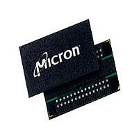
MT47H128M8HQ-3 L:G Micron Technology Inc, MT47H128M8HQ-3 L:G Datasheet - Page 85

MT47H128M8HQ-3 L:G
Manufacturer Part Number
MT47H128M8HQ-3 L:G
Description
IC DDR2 SDRAM 1GBIT 3NS 60FBGA
Manufacturer
Micron Technology Inc
Type
DDR2 SDRAMr
Specifications of MT47H128M8HQ-3 L:G
Format - Memory
RAM
Memory Type
DDR2 SDRAM
Memory Size
1G (128M x 8)
Speed
3ns
Interface
Parallel
Voltage - Supply
1.7 V ~ 1.9 V
Operating Temperature
0°C ~ 85°C
Package / Case
60-FBGA
Organization
128Mx8
Density
1Gb
Address Bus
17b
Access Time (max)
450ps
Maximum Clock Rate
667MHz
Operating Supply Voltage (typ)
1.8V
Package Type
FBGA
Operating Temp Range
0C to 85C
Operating Supply Voltage (max)
1.9V
Operating Supply Voltage (min)
1.7V
Supply Current
135mA
Pin Count
60
Mounting
Surface Mount
Operating Temperature Classification
Commercial
Lead Free Status / RoHS Status
Lead free / RoHS Compliant
- Current page: 85 of 131
- Download datasheet (10Mb)
Initialization
Figure 42: DDR2 Power-Up and Initialization
DDR2 SDRAM must be powered up and initialized in a predefined manner. Operational procedures other than those specified may result in unde-
fined operation. Figure 42 illustrates, and the notes outline, the sequence required for power-up and initialization.
Command
Address
DQS
DM
DQ
V
V
V
ODT
V
V
CK#
CKE
DDQ
DDL
R
TT
CK
REF
DD
15
16
15
15
tt
1
low level 2
LVCMOS
High-Z
High-Z
High-Z
t
VTD 1
T0
t CL
V
clock (CK, CK#)
low level
T = 200µs (MIN) 3
Power-up:
SSTL_18
DD
t CK
and stable
t CL
2
NOP 3
Ta0
T = 400ns (MIN) 4
A10 = 1
Tb0
PRE
t RPA
EMR(2)
LM 5
Code
Tc0
t MRD
EMR(3)
Code
LM 6
Td0
t MRD
Code
LM 7
EMR
Te0
t MRD
DLL RESET
MR with
Code
LM 8
Tf0
t MRD
A10 = 1
PRE 9
Tg0
t RPA
200 cycles of CK are required before a READ command can be issued
REF 10
Th0
t RFC
See no te 10
REF 10
Ti0
t RFC
MR without
DLL RESET
LM 11
Code
Tj0
t MRD
OCD default
EMR with
LM 12
Code
Tk0
Indicates a Break in
Time Scale
t MRD
EMR with
OCD exit
LM 13
Code
Tl0
t MRD
operation
Don’t care
Normal
Valid 14
Valid
Tm0
Related parts for MT47H128M8HQ-3 L:G
Image
Part Number
Description
Manufacturer
Datasheet
Request
R

Part Number:
Description:
IC SDRAM 64MBIT 133MHZ 54TSOP
Manufacturer:
Micron Technology Inc
Datasheet:

Part Number:
Description:
IC SDRAM 64MBIT 5.5NS 86TSOP
Manufacturer:
Micron Technology Inc
Datasheet:

Part Number:
Description:
IC SDRAM 64MBIT 200MHZ 86TSOP
Manufacturer:
Micron Technology Inc
Datasheet:

Part Number:
Description:
IC SDRAM 64MBIT 133MHZ 54TSOP
Manufacturer:
Micron Technology Inc
Datasheet:

Part Number:
Description:
IC SDRAM 128MBIT 133MHZ 54TSOP
Manufacturer:
Micron Technology Inc
Datasheet:

Part Number:
Description:
IC SDRAM 256MBIT 133MHZ 90VFBGA
Manufacturer:
Micron Technology Inc
Datasheet:

Part Number:
Description:
IC SDRAM 128MBIT 133MHZ 54TSOP
Manufacturer:
Micron Technology Inc
Datasheet:

Part Number:
Description:
IC SDRAM 256MBIT 133MHZ 54TSOP
Manufacturer:
Micron Technology Inc
Datasheet:

Part Number:
Description:
IC DDR SDRAM 512MBIT 6NS 66TSOP
Manufacturer:
Micron Technology Inc
Datasheet:

Part Number:
Description:
IC SDRAM 128MBIT 167MHZ 86TSOP
Manufacturer:
Micron Technology Inc
Datasheet:

Part Number:
Description:
IC SDRAM 128MBIT 143MHZ 86TSOP
Manufacturer:
Micron Technology Inc
Datasheet:

Part Number:
Description:
SDRAM 256M-BIT 1.8V 54-PIN VFBGA
Manufacturer:
Micron Technology Inc
Datasheet:

Part Number:
Description:
IC SDRAM 128MBIT 143MHZ 86TSOP
Manufacturer:
Micron Technology Inc
Datasheet:

Part Number:
Description:
IC SDRAM 128MBIT 125MHZ 54VFBGA
Manufacturer:
Micron Technology Inc
Datasheet:

Part Number:
Description:
IC SDRAM 128MBIT 125MHZ 54VFBGA
Manufacturer:
Micron Technology Inc
Datasheet:


