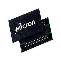
MT47H128M8HQ-3 L:G Micron Technology Inc, MT47H128M8HQ-3 L:G Datasheet - Page 46

MT47H128M8HQ-3 L:G
Manufacturer Part Number
MT47H128M8HQ-3 L:G
Description
IC DDR2 SDRAM 1GBIT 3NS 60FBGA
Manufacturer
Micron Technology Inc
Type
DDR2 SDRAMr
Specifications of MT47H128M8HQ-3 L:G
Format - Memory
RAM
Memory Type
DDR2 SDRAM
Memory Size
1G (128M x 8)
Speed
3ns
Interface
Parallel
Voltage - Supply
1.7 V ~ 1.9 V
Operating Temperature
0°C ~ 85°C
Package / Case
60-FBGA
Organization
128Mx8
Density
1Gb
Address Bus
17b
Access Time (max)
450ps
Maximum Clock Rate
667MHz
Operating Supply Voltage (typ)
1.8V
Package Type
FBGA
Operating Temp Range
0C to 85C
Operating Supply Voltage (max)
1.9V
Operating Supply Voltage (min)
1.7V
Supply Current
135mA
Pin Count
60
Mounting
Surface Mount
Operating Temperature Classification
Commercial
Lead Free Status / RoHS Status
Lead free / RoHS Compliant
Output Electrical Characteristics and Operating Conditions
Table 17: Differential AC Output Parameters
Figure 14: Differential Output Signal Levels
Table 18: Output DC Current Drive
PDF: 09005aef821ae8bf
1GbDDR2.pdf – Rev. T 02/10 EN
Parameter
AC differential cross-point voltage
AC differential voltage swing
Parameter
Output MIN source DC current
Output MIN sink DC current
Notes:
Note:
V
V
TR
CP
1. The typical value of V
1. For I
2. For I
3. The DC value of V
4. The values of I
vice and V
which differential output signals must cross.
values of V
between 0V and 280mV.
are used to test device drive current capability to ensure V
V
ues are derived by shifting the desired driver operating point (see output IV curves)
along a 21Ω load line to define a convenient driver current for measurement.
IL,max
Output Electrical Characteristics and Operating Conditions
OH(DC)
OL(DC)
minus a noise margin are delivered to an SSTL_18 receiver. The actual current val-
; V
; V
OX(AC)
OUT
V
V
DDQ
DDQ
DDQ
Symbol
SSQ
Vswing
V
Vswing
OH(DC)
between V
OX(AC)
is expected to track variations in V
= 1.7V, V
= 1.7V, V
REF
and I
applied to the receiving device is set to V
OX(AC)
OUT
OL(DC)
OUT
DDQ
46
0.50 × V
is expected to be about 0.5 × V
= 280mV. V
= 1,420mV. (V
Crossing point
and V
are based on the conditions given in Notes 1 and 2. They
Min
Symbol
1.0
DDQ
V
I
I
DDQ
OH
OX
OL
Micron Technology, Inc. reserves the right to change products or specifications without notice.
- 125
- 280mV.
OUT
OUT
/I
1Gb: x4, x8, x16 DDR2 SDRAM
OL
- V
must be less than 21Ω for values of V
0.50 × V
Value
DDQ
–13.4
DDQ
13.4
)/I
. V
OH
Max
OX(AC)
DDQ
–
IH,min
DDQ
must be less than 21Ω for
© 2004 Micron Technology, Inc. All rights reserved.
+ 125
TT
of the transmitting de-
indicates the voltage at
plus a noise margin and
.
Units
mA
mA
Units
mV
mV
Notes
1, 2, 4
2, 3, 4
Notes
1
OUT


