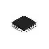
L6711TR STMicroelectronics, L6711TR Datasheet - Page 10

L6711TR
Manufacturer Part Number
L6711TR
Description
IC CTRLR 3PHASE VID/DACS 48-TQFP
Manufacturer
STMicroelectronics
Type
Step-Down (Buck)r
Datasheet
1.L6711TR.pdf
(50 pages)
Specifications of L6711TR
Internal Switch(s)
No
Synchronous Rectifier
No
Number Of Outputs
1
Voltage - Output
0.8 ~ 1.55 V
Current - Output
2A
Frequency - Switching
150kHz
Voltage - Input
12V
Operating Temperature
0°C ~ 70°C
Mounting Type
Surface Mount
Package / Case
48-TQFP Exposed Pad, 48-eTQFP, 48-HTQFP, 48-VQFP
Power - Output
2.5W
Output Voltage
0.8 V to 1.581 V
Output Current
95 A
Input Voltage
13.8 V
Mounting Style
SMD/SMT
Maximum Operating Temperature
+ 125 C
Minimum Operating Temperature
0 C
Lead Free Status / RoHS Status
Lead free / RoHS Compliant
Other names
497-5363-2
L6711TR
L6711TR
Available stocks
Company
Part Number
Manufacturer
Quantity
Price
Pins description and connection diagrams
Table 1.
10/50
23, 24
to 28
N°
29
30
31
32
33
34
35
36
37
38
39
40
41
42
43
44
VID_SEL
VCCDR3
VCCDR2
SS_END
PHASE3
UGATE3
PHASE2
UGATE2
LGATE3
LGATE2
PGND3
PGND2
BOOT3
BOOT2
VID0-4
SGND
Name
VID5,
N.C.
Pins description
Voltage IDentification pins.
Internally pulled-up to 3V, connect to SGND to program a logic ‘0’ while leave floating (as well
as pull-up with a resistor up to 3.3V) to program a logic ‘1’.
They are used to program the output voltage as specified in
VID_SEL and to set the OVP/UVP protection thresholds accordingly.
See relevant section for details about DAC selection.
VID_SELect pin. Through this pin it is possible to select the DAC table used for the regulation.
Leave floating to use a VRD10.x compliant DAC (See
VRM-Hammer compliant DAC (See
See relevant section for details about DAC selection.
Soft start end signal. It is an open collector output, set free after finishing the soft start.
Pull-up with a resistor to a voltage lower than 5V, if not used may be left floating.
All the internal references are referred to this pin. Connect it to the PCB signal ground.
Channel 3 HS driver return path. It must be connected to the HS3 mosfet source and provides
the return path for the HS driver of channel 3.
Channel 3 HS driver output.
A little series resistor helps in reducing device-dissipated power.
Channel 3 HS driver supply. This pin supplies the relative high side driver.
Connect through a capacitor (100nF Typ.) to the PHASE3 pin and through a diode to VCC
(cathode vs. boot).
Channel 3 LS driver return path.
Connect to Power Ground Plane.
Channel 3 LS driver output.
A little series resistor helps in reducing device-dissipated power.
Not internally connected.
Channel 3 LS driver supply: it can be varied from 5V to 12V buses.
It must be connected together with other VCCDRx pins.
Filter locally with at least 1 F ceramic cap vs. PGND3.
Channel 2 LS driver return path.
Connect to Power Ground Plane.
Channel 2 LS driver output.
A little series resistor helps in reducing device-dissipated power.
Channel 2 LS driver supply: it can be varied from 5V to 12V buses.
It must be connected together with other VCCDRx pins.
Filter locally with at least 1 F ceramic cap vs. PGND2.
Channel 2 HS driver return path. It must be connected to the HS2 mosfet source and provides
the return path for the HS driver of channel 2.
Channel 2 HS driver output.
A little series resistor helps in reducing device-dissipated power.
Channel 2 HS driver supply. This pin supplies the relative high side driver.
Connect through a capacitor (100nF Typ.) to the PHASE2 pin and through a diode to VCC
(cathode vs. boot).
(continued)
Table
Description
3).
Table
Table 5
1) while short to SGND to use a
and
Table 6
together with
L6711


