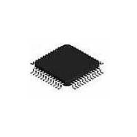
L6711TR STMicroelectronics, L6711TR Datasheet - Page 22

L6711TR
Manufacturer Part Number
L6711TR
Description
IC CTRLR 3PHASE VID/DACS 48-TQFP
Manufacturer
STMicroelectronics
Type
Step-Down (Buck)r
Datasheet
1.L6711TR.pdf
(50 pages)
Specifications of L6711TR
Internal Switch(s)
No
Synchronous Rectifier
No
Number Of Outputs
1
Voltage - Output
0.8 ~ 1.55 V
Current - Output
2A
Frequency - Switching
150kHz
Voltage - Input
12V
Operating Temperature
0°C ~ 70°C
Mounting Type
Surface Mount
Package / Case
48-TQFP Exposed Pad, 48-eTQFP, 48-HTQFP, 48-VQFP
Power - Output
2.5W
Output Voltage
0.8 V to 1.581 V
Output Current
95 A
Input Voltage
13.8 V
Mounting Style
SMD/SMT
Maximum Operating Temperature
+ 125 C
Minimum Operating Temperature
0 C
Lead Free Status / RoHS Status
Lead free / RoHS Compliant
Other names
497-5363-2
L6711TR
L6711TR
Available stocks
Company
Part Number
Manufacturer
Quantity
Price
DAC Selection
8
22/50
The device embeds a selectable DAC that allows the output voltage to have a tolerance of
±0.5% (0.6% for Hammer DAC) recovering from offsets and manufacturing variations. The
VID_SEL pin selects the DAC table used to program the reference for the regulation as
shown in
Table 7.
VID pins are inputs of an internal DAC that is realized by means of a series of resistors
providing a partition of the internal voltage reference. The VID code drives a multiplexer that
selects a voltage on a precise point of the divider. The DAC output is delivered to an
amplifier obtaining the voltage reference (i.e. the set-point of the error amplifier, V
Internal pull-ups are provided (realized with a 5 A current generator up to 3V Typ); in this
way, to program a logic "1" it is enough to leave the pin floating, while to program a logic "0"
it is enough to short the pin to SGND.
Programming the "11111x" code (NOCPU, VID5 is irrelevant), the device shuts down: all
mosfets are turned OFF and SS_END is shorted to SGND. Removing the code causes the
device to restart.
The voltage identification (VID) pin configuration also sets the Over / Under Voltage
protection (OVP/UVP) thresholds.
DAC Selection
VID_SEL
OPEN
SGND
Table
VRM / VRD 10.x DAC.
Output voltage ranges from 0.8185V to 1.5810V with 12.5mV steps (See
Since the VIDx pins program the maximum output voltage, according to VRD 10.x
specs, the device automatically regulates with –19mV offset avoiding use of any external
component to lower the regulated voltage.
Since the -19mV offset is programmed during the production stage, no further error is
introduced to generate the offset since it is automatically recovered during the trimming
stage.
SGND
OPEN
DAC Selection
VID5
.
Output voltage ranges from 0.800V to 1.550V with 25mV steps (See
Output voltage ranges from 0.825V to 1.575V with 25mV steps (See
Since the +25mV offset is programmed during the production stage, no further
error is introduced to generate the offset since it is automatically recovered
during the trimming stage.
Selected DAC
Hammer DAC
Table
PROG
Table
Table
5).
L6711
).
6).
6).


