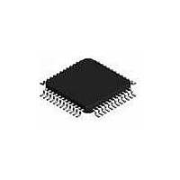
L6711TR STMicroelectronics, L6711TR Datasheet - Page 9

L6711TR
Manufacturer Part Number
L6711TR
Description
IC CTRLR 3PHASE VID/DACS 48-TQFP
Manufacturer
STMicroelectronics
Type
Step-Down (Buck)r
Datasheet
1.L6711TR.pdf
(50 pages)
Specifications of L6711TR
Internal Switch(s)
No
Synchronous Rectifier
No
Number Of Outputs
1
Voltage - Output
0.8 ~ 1.55 V
Current - Output
2A
Frequency - Switching
150kHz
Voltage - Input
12V
Operating Temperature
0°C ~ 70°C
Mounting Type
Surface Mount
Package / Case
48-TQFP Exposed Pad, 48-eTQFP, 48-HTQFP, 48-VQFP
Power - Output
2.5W
Output Voltage
0.8 V to 1.581 V
Output Current
95 A
Input Voltage
13.8 V
Mounting Style
SMD/SMT
Maximum Operating Temperature
+ 125 C
Minimum Operating Temperature
0 C
Lead Free Status / RoHS Status
Lead free / RoHS Compliant
Other names
497-5363-2
L6711TR
L6711TR
Available stocks
Company
Part Number
Manufacturer
Quantity
Price
L6711
Table 1.
N°
17
18
19
20
21
22
CS_SEL
FAULT
Name
OSC /
CS2+
CS3+
CS3-
TC
Pins description
Channel 2 Current Sense Positive Input pin.
It must be connected through an Rg resistor to the LS mosfet source (or to the GND-side of
the sense resistor placed in series to the LS mosfet) if LS mosfet sense is performed
(CS_SEL=OPEN). Otherwise (CS_SEL=SGND), it must be connected to the phase-side of
the output inductor (or the inductor-side of the sense resistor used and placed between the
channel 2 inductor and the output of the converter) through Rg resistor and an R-C network
across the inductor.
The net connecting the pin to the sense point must be routed as close as possible to the CS2-
net in order to couple in common mode any picked-up noise.
Channel 3 Current Sense Negative Input pin.
It must be connected through an Rg resistor to the LS mosfet drain (or to the LS-side of the
sense resistor placed in series to the LS mosfet) if LS mosfet sense is performed
(CS_SEL=OPEN). Otherwise (CS_SEL=SGND), it must be connected to the output-side of
the output inductor (or the output-side of the sense resistor used and placed between the
channel 3 inductor and the output of the converter) through Rg resistor.
The net connecting the pin to the sense point must be routed as close as possible to the CS3+
net in order to couple in common mode any picked-up noise.
Channel 3 Current Sense Positive Input pin.
It must be connected through an Rg resistor to the LS mosfet source (or to the GND-side of
the sense resistor placed in series to the LS mosfet) if LS mosfet sense is performed
(CS_SEL=OPEN). Otherwise (CS_SEL=SGND), it must be connected to the phase-side of
the output inductor (or the inductor-side of the sense resistor used and placed between the
channel 3 inductor and the output of the converter) through Rg resistor and an R-C network
across the inductor.
The net connecting the pin to the sense point must be routed as close as possible to the CS3-
net in order to couple in common mode any picked-up noise.
Temperature Compensation pin.
Connect through a resistor R
compensation effect.
Short to SGND to disable the compensation effect.
Current Reading Selection pin, internally 5V pulled-up.
Leave floating to sense current across low-side mosfets or a sense resistor placed in series to
the LS mosfet source. Maximum duty cycle is dynamically limited and Track&Hold is enabled
to assure proper reading of the current.
Short to SGND to read current across inductors or a sense resistor placed in series to the
output inductors. No duty cycle limitation and no Track&Hold performed in this case.
Oscillator pin.
It allows programming the switching frequency of each channel: the equivalent switching
frequency at the load side results in being tripled.
Internally fixed at 1.24V, the frequency is varied proportionally to the current sunk (forced)
from (into) the pin with an internal gain of 6kHz/ A (See relevant section for details).
If the pin is not connected, the switching frequency is 150kHz for each channel (450kHz on the
load).
The pin is forced high (5V Typ.) when an Over/Under Voltage is detected; to recover from this
condition, cycle VCC or the OUTEN pin.
(continued)
TC
and filter with 10nF vs. SGND to program the temperature
Description
Pins description and connection diagrams
9/50


