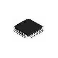
L6711TR STMicroelectronics, L6711TR Datasheet - Page 19

L6711TR
Manufacturer Part Number
L6711TR
Description
IC CTRLR 3PHASE VID/DACS 48-TQFP
Manufacturer
STMicroelectronics
Type
Step-Down (Buck)r
Datasheet
1.L6711TR.pdf
(50 pages)
Specifications of L6711TR
Internal Switch(s)
No
Synchronous Rectifier
No
Number Of Outputs
1
Voltage - Output
0.8 ~ 1.55 V
Current - Output
2A
Frequency - Switching
150kHz
Voltage - Input
12V
Operating Temperature
0°C ~ 70°C
Mounting Type
Surface Mount
Package / Case
48-TQFP Exposed Pad, 48-eTQFP, 48-HTQFP, 48-VQFP
Power - Output
2.5W
Output Voltage
0.8 V to 1.581 V
Output Current
95 A
Input Voltage
13.8 V
Mounting Style
SMD/SMT
Maximum Operating Temperature
+ 125 C
Minimum Operating Temperature
0 C
Lead Free Status / RoHS Status
Lead free / RoHS Compliant
Other names
497-5363-2
L6711TR
L6711TR
Available stocks
Company
Part Number
Manufacturer
Quantity
Price
L6711
7
7.1
Current reading and current sharing control loop
The device embeds a flexible, fully-differential current sense circuitry that is able to read
across both low side or inductor parasitic resistance or across a sense resistor placed in
series to that element. The fully-differential current reading rejects noise and allows placing
sensing element in different locations without affecting the measurement's accuracy. The
kind of sense element can be simply chosen through the CS_SEL pin: setting this pin free,
the LS mosfet is used while shorting it to SGND, the inductor will be used instead. Details
about connections are shown in
The high bandwidth current sharing control loop allows current balance even during load
transients: a current reference equal to the average of the read current (I
built and the error between the read current and this reference is converted to a voltage that
with a proper gain is used to adjust the duty cycle whose dominant value is set by the
voltage error amplifier.
Figure 5.
Low-side current reading
Leaving CS_SEL pin OPEN, the current flowing trough each phase is read using the voltage
drop across the low side mosfets R
internally converted into a current. The transconductance ratio is issued by the external
resistor Rg placed outside the chip between CSx- and CSx+ pins toward the reading points
(see
time T
conduction time (OFF Time, see
rest of the period.
This device sources a constant 50 A current from the CSx+ pin: the current reading circuitry
uses this pin as a reference and the reaction keeps the CSx- pin to this voltage during the
reading time (an internal clamp keeps CSx+ and CSx- at the same voltage sinking from the
CSx- pin the necessary current during the hold time; this is needed when LS mosfet R
sense is implemented to avoid absolute maximum rating overcome on CSx- pin). The
current that flows from the CSx- pin is then given by the following equation (See
right):
R
used between CSx- and CSx+ pins toward the reading points; I
by the relative phase and I
I
CSx-
dsON
Figure 6
=
TRACK
is the on resistance of the low side mosfet and Rg is the transconductance resistor
50 A
LGATEx
CS_SEL
CSx+
CSx-
LS MOSFET Current Sense
= T
Current reading connections selectable through CS_SEL pin.
+
right). The proprietary current sense circuit tracks the current information for a
R
---------------- - I
SW
dsON
R
g
/3 (T
Rg
Rg
PHASEx
SW
INFOx
= 1/F
I
PHASE
=
SW
is the current information signal reproduced internally.
Figure
Figure 6
50 A
) centered in the middle of the low-side mosfet
dsON
Current reading and current sharing control loop
+
5.
or across a sense resistor in its series and it is
I
INFOx
left) and holds the tracked information during the
where:
PHASEx
CS_SEL
C Sx+
CSx-
Inductor Current Sense
I
INFOx
R
R g
g(a)
=
PHASEx
R
---------------- - I
dsON
R
g
R
g(R C)
I
L
P HA SE
C
is the current carried
g
PHASEx
AVG
R
L
) is internally
OU T
Figure 6 -
dsON
19/50


